


Next: 4.5.3 Sub-Pixel Position Reconstruction Up: 4.5 Instrument Performance Models Previous: 4.5.1 CCD Interaction Simulation
Next: 4.5.3 Sub-Pixel Position Reconstruction
Up: 4.5 Instrument Performance Models
Previous: 4.5.1 CCD Interaction Simulation
 |
 |
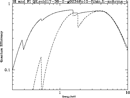
As previously mentioned, ACIS will employ CCDs in two fundamentally
different operating configurations. Some devices will be used
with the surface containing the gate structures facing the incident
X-ray beam from the HRMA. This is the normal CCD operating configuration,
and is called `Frontside Illumination' (FI). Unfortunately the
gate structures are required for electrical reasons to have a substantial
thickness (![]() 4000 Å) which leads to a reduction in the low
energy quantum efficiency of the device.
4000 Å) which leads to a reduction in the low
energy quantum efficiency of the device.
An alternative is to remove the substrate silicon from the back of
the device, exposing the active sensing volume (the depletion layer)
from the back side of the device. This configuration is called
`Backside Illumination' (BI). While BI chips have higher low energy
quantum efficiency, they have somewhat lower total high energy quantum
efficiency due to a lower thickness![[*]](/images/LatexHtml/foot_motif.gif) . More importantly BI
chips are harder to make, in that the additional processing required
to make a BI chip from a potential FI parent has a loss associated
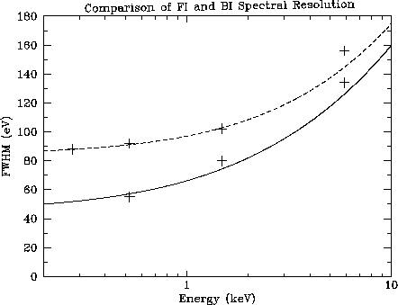
with it, and lab measurements show that BI chips do not approach
theoretical energy resolution as the FI chips do.
. More importantly BI
chips are harder to make, in that the additional processing required
to make a BI chip from a potential FI parent has a loss associated
with it, and lab measurements show that BI chips do not approach
theoretical energy resolution as the FI chips do.
The advantages of the BI chips are particularly important for applications using the gratings, as the improved quantum efficiency at low energy is very important and the loss of energy resolution is less important because the CCD energy resolution is only used to separate orders, and not measure energy directly. Fig. 4.13 compares the quantum efficiency of BI and FI chips on a wavelength scale (which corresponds to linear spatial location along the grating dispersion direction).
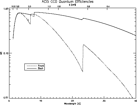 |
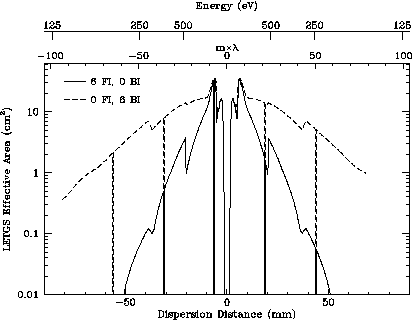
Fig. 4.14 shows the net effective area of ACIS-S when all CCDs are BI (broken line) and all CCDs are FI (solid line). The gain at energies below 1 keV is dramatic.
 |
John Nousek