Next: 4.5.2 Frontside vs. Backside Up: 4.5 Instrument Performance Models Previous: 4.5 Instrument Performance Models
![]()
![]()
![]()
![]()

Next: 4.5.2 Frontside vs. Backside
Up: 4.5 Instrument Performance Models
Previous: 4.5 Instrument Performance Models
In a back-illuminated device, the top layer is a damage or surface layer, in which liberated charge is not efficiently propagated and is largely lost to recombination. Photons which interact in this layer may only have about 20% of their charge propagated to the depletion layer. Below this damaged or ``modified substrate'' layer is a field-free layer, which acts as a reflecting layer and prevents charge from the depletion region from leaking out into the modified substrate and generating dark current. The surface and field-free layers sit on top of the depletion layer, which ends in the buried channel and gate structure at the bottom of the device.
An epitaxial front-illuminated device is similar to an inverted back-illuminated device. The top layer is the gate structure, modeled simply as a uniform slab of absorbing material (a ``dead'' layer). Beneath this is the depletion region, followed by a field-free region, then a substrate. The bulk front-illuminated device has the same dead layer on top of a depletion layer, but this is simply followed by a substrate.
In order to simulate X-ray photon detection by these devices, a random interaction depth and position on the CCD are generated for each simulated photon. The photon is allowed to interact with the device and produce a cloud of charge. This charge spreads through the layers of the device, with the spreading rate and the charge reflection and absorption dependent on the properties of each layer. Once the charge reaches the buried channel, it is ``detected'' by recording an appropriate number of electrons in each pixel over which the charge spread. The degree to which a given photon's charge cloud is split across pixels depends on the photon's energy, its interaction depth, and the proximity of the interaction to pixel boundaries.
The simulation accounts for the possibility of secondary fluorescent photon generation from the silicon, if the initial photon energy is high enough. Fluorescent photons from other elements in the device (such as oxygen) may occur, but with a lower probability, so they have not been included in the simulation at this time. As the charge cloud propagates through the device, some of the charge may recombine and be lost. This charge recombination has been estimated empirically and is included in the model.
The output of the simulation is a square CCD frame, with the size determined by the user. It is in units of electrons and contains photon events, readout and other noise, and minimally-ionizing particle events. These particle events were modeled similarly to photon events; the track of a particle through the detector is randomly generated, then simulated by allowing the detector to absorb energy from the particle every time it traverses one micron in depth through the device. The charge cloud generated at each interaction point is propagated just as photon charge clouds are propagated.
 |
 |
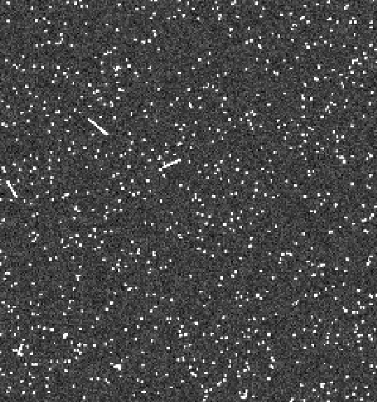
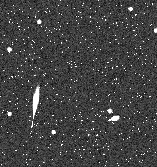
Figure 4.9 shows the output for a back-illuminated device with 1000 1 keV photon events and 10 particle events. Note that most of the photon events are spread among several pixels at this energy. For comparison, consider Figure 4.10, which also contains 1000 1 keV photon event and 10 particle events, but detected by a front-illuminated device. Most of the photon events are contained in a single pixel. Note how much more the particle events have bloomed - this is a result of the thick substrate assumed for this device.
Radiation damage may also be included in the model, manifested by increased charge transfer inefficiency. This effect may have a power-law dependence with energy. The code allows the user to supply this power and the CTI.
The assumptions made in this X-ray CCD frame simulator limit its ability to reproduce actual CCD output. Several enhancements are possible. The complex geometry of the gate structure and the channel stops should be included, especially for front-illuminated devices where photons must pass through these top layers of the detector in order to be recognized. The Fano factor (the conversion factor giving the number of eV's per electron) may be temperature and energy dependent. Once an empirical estimate of these dependencies is available, it should be incorporated into the algorithm. As mentioned above, other elements (besides silicon) present in the CCD can produce fluorescent photons. The most predominant two or three of these fluorescent lines should be included in the simulation (but note that the rates will be even lower than the 4% fluorescence rate for silicon). Currently only one dopant concentration is considered; it may be more realistic to allow different dopant concentrations for different device layers.
In spite of its limitations, the current incarnation of the frame simulator is useful for addressing timely issues in CCD characterization. The code has been used to develop an algorithm to determine sub-pixel positions of photons and to assess the problems associated with photon pile-up from bright uniform beams and bright point sources. It also should be useful in modeling flickering pixels and addressing the ``sacrificial photon'' problem in modeling the CTI.
The ``sacrificial photon'' problem occurs when the CTI is poor and a high incident flux of photons strikes the detector. The poor CTI results from traps removing electrons from the X-ray induced charge packet as it is clocked across the CCD. These traps have trapping times for electrons comparable to the row readout time. (If the trapping time were short compared to the pixel clocking time, then the trap would lose the electron and not affect the packet. If the trapping time were long, then the trap would stay filled and the CTI would disappear.)
If two photons strike the CCD row closely enough in time for the second packet to arrive before all the electrons from the first packet are re-emitted, then the trapping capacity is less for the second photon than the first (or sacrificial) photon which gave up the full charge.
The key point is that the observed charge may no longer be strictly linear with incident X-ray energy, but may have a rate dependent effect. The effects of sacrificial photons can be modeled by the full frame X-ray interaction simulator which we described, which can not be handled by any simulator which treats each X-ray interaction as independent.

John Nousek