 Table of Contents
 Previous Chapter
Table of Contents
Previous Chapter
This section describes the hardware-to-software interfaces of the ACIS Digital Processor Assembly (DPA), and describes the software design elements which are responsible for managing these interfaces. The DPA contains two types of processors: a Back End Processor (BEP), and a collection of 6 Front End Processors (FEP). The next two subsection describe the BEP and FEP interfaces.
The ACIS Digital Processor Assembly contains a primary and backup Back End Processor (BEP). The ground commands the hardware to power up only one Back End Processor at a time. The ACIS Science Instrument Software has no direct knowledge of this redundancy.
This section describes the overall BEP interrupts and priorities provided by the BEP hardware, describes the Boot ROM, and then describes the key interfaces provided by the hardware. The hardware memory map of the BEP is shown by Table 55, "Back End Virtual Memory Map," on page 86.
The BEP hardware provides the following interfaces to the software running on the processor:
In addition to these interfaces, the Mongoose Microcontroller provides the following devices:
Refer to the Mongoose ASIC Microcontroller Programming Guide for a description of the interfaces to these devices.
This section identifies the interrupts supported by the Back End Processor and identifies the top level units responsible for handling interrupts. Table 2 lists the key interrupt causes.
 TABLE 2. Back End Interrupt Cause List
---------------------------------------------------------------------- Name Device---------------------------------------------------------------------- Command Interface BEP Command Interface Telemetry Transfer Complete BEP Telemetry DTC FEP Interrupt BEP's FEP I/O Interfaces Write Bus Error Mongoose - Memory Bus DMA Bus Error Mongoose - DMA Data Read Bus Error Mongoose - Memory Bus Instruction Read Bus Error Mongoose - I-cache External Memory Bus Error Mongoose - Memory Bus UART TX Ready Mongoose - UART UART RX Ready Mongoose - UART DMA Done Mongoose - DMA General Purpose Timer (Timer 2) End of Count Mongoose - Timer 2 Watchdog Timer (Timer 1) End of Count Mongoose - Timer 1 ----------------------------------------------------------------------
All interrupts cause the processor to branch to the General Exception Vector. This vector then branches to a common interrupt and exception handler. This handler then examines the R3000's System Coprocessor's (CP0) Cause Register and the Mongoose's XCause Register to determine the pending interrupts and exceptions. The software then handles each of the pending conditions, as described later in this section.
The ACIS's Back End Processor handler will first deal with all error conditions which may have caused the interrupt. It then will deal with device interrupts in the following order:
1. UART RX Ready (Debug Only)
2. UART TX Ready (Debug Only)
3. Watchdog Timer (Debug Only, since this will cause a reset in-flight)
4. Command Interface Interrupt
5. Telemetry Transfer Complete Interrupt
6. Science Frame Interrupt
7. General Purpose Timer Interrupt
8. Front End Processor (FEP) Interrupt
9. Mongoose DMA Done Interrupt
In flight, the Command and Telemetry Interface interrupts are handled at the highest priority in order to allow the possibility of diagnosing problems during handling of lower priority interrupts. The timer interrupts are handled at the next level to help ensure that they are handled before the next tick occurs. The time to handle command, telemetry and timing interrupts must be less than the fastest timer tick responded to by the system. The order of the remaining interrupt priorities is designed to help maintain the throughput of the science data within the system.
Figure 7 illustrates interrupt handling in the Back End software.
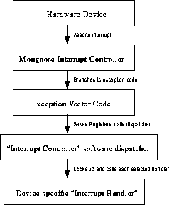
Each interrupt cause is managed using an "Interrupt Handler" class, which provides a generic interface from the rest of the software to the interrupt handling system. This class provides the operations listed in Table 3.
TABLE 3. `Interrupt Handler'Operations
--------------------------------- Function Inputs Outputs--------------------------------- Initialize none none Handle Interrupt none none ---------------------------------
Control is passed to a handler by the common interrupt dispatcher, "Interrupt Controller." This class provides the operations listed in Table 4.
TABLE 4. `Interrupt Controller'Operations
---------------------------------------------------------------------------- Function Inputs Outputs---------------------------------------------------------------------------- Initialize none none Disable none Disables all interrupts and returns previous interrupt state Enable none Enable interrupts Handle Interrupt Interrupt Cause Mask Calls each interrupt handler asso ciated with all pending interrupts in the "mask" ----------------------------------------------------------------------------
As described earlier, when a device asserts an interrupt, the Mongoose Interrupt controller passes control to the code located at the Exception Vector Address. This code saves the processor registers, tells the real-time executive to save its state, retrieves the Interrupt Cause registers, and branches to a common handler routine, coupled to an "Interrupt Controller" class. This routine works through each of the causes of the interrupt, using each cause as an index into an array of "Interrupt Handler" pointers. For each asserted interrupt cause, it fetches the corresponding pointer and invokes its "Handle Interrupt" routine. The "Handle Interrupt" routine then performs whatever device-specific operations need to be performed (including signaling applicable tasks when appropriate), and returns to the dispatcher, which then tells the real-time executive to restore its state. It then returns to the Exception Vector code, which, in turn, returns control to the code which was interrupted or which has been scheduled by the real-time executive's context switcher.
The Back End Processor's Boot ROM starts at memory location 0x0BFC00000 and contains 32Kbytes of ROM (see Table 55, "Back End Virtual Memory Map," on page 86). The contents of this ROM are as follows:
The Microboot Word is located within the Boot ROM at virtual address 0x0BFFFFFFC. This word controls the chip-select and decode address for the instruction and data cache RAM chips. This address will map to the last 4 byte location within the 32Kbyte Boot ROM. Upon processor reset, the Mongoose hardware fetches this word and uses it to configure its internal memory cache control logic. The Mongoose then sets its program counter to the Boot Reset Vector.
The Boot Reset Vector is located in the Boot ROM at virtual address 0xBFC00000. Upon reset, the Mongoose executes the instructions located at this address. Typically, these instructions will immediately branch to the Boot ROM initialization code.
Since the Mongoose Processor does not contain a Translation Lookaside Buffer (TLB), the Boot UTLB Exception Vector is not used by the Mongoose Processor.
The Boot Exception Vector is located in the Boot ROM at virtual address 0xBFC00080. Upon reset, the Boot Exception Vector Bit (BEV) (contained in the R3000's System Coprocessor's Status Register) will be asserted. If the Mongoose receives an exception or interrupt while booting up (as indicated by the BEV bit), it saves the current program counter in the R3000's Exception Program Counter (EPC) register and branches to the code located at this address. Typically, this code then jumps to the Boot ROM's exception handling code.
(NOTE: Once the application code is loaded and executed, it must load its own exception handling code into RAM and de-assert the BEV bit).
Upon reset of the Back End Processor, the boot-strap Executable Code is invoked by the instructions located at the Boot Reset Vector. The boot-strap code proceeds to initialize the processor registers. It then loads and executes code and data from either the Back End Processor Software ROM, or from a series of command packets read from the Command Interface.
Given the stable requirements and simple interfaces of the boot-strap loader, the Back End Processor's Boot ROM software will be designed using top-down techniques, and will be implemented using MIPS Assembler and "C."
The Back End Processor (BEP) hardware presents the software with two types of command interfaces, discrete command flags and serial digital software commands. The discrete command flags are provided to the software in the form of status bits, read from a TBD BEP status register. These include the Load from Uplink Flag, the Radiation Monitor Flag, and the Standby Flag.
Serial digital software commands are sent to ACIS in the form of Command Packets. Each Command Packet contains a list of 16-bit words (256 maximum). The first word in each list contains the number of words in the packet. As each word is received from the RCTU, the BEP hardware writes the word into a command FIFO. On the first word of each packet, the hardware copies the first word into a packet word counter. Each write to the FIFO (including the write of the length word) then decrements the counter. Once all words from a packet have been written into the FIFO, the counter reaches zero and the hardware generates a Command Interrupt. The software then reads the packet from the FIFO and forwards the packet to a command task for execution.
If the command FIFO fills, there is no way for the software to determine if any command words were lost. The software treats a FIFO full condition as an error. If the FIFO becomes full, or if the hardware detects an illegal packet length (i.e. a length greater than 256 words), it sets an appropriate error bit in a command status register and generates a Command Interrupt. The software then attempts to recover from the error and locate the start of the next Command Packet.
Table 5 lists the software operations and status of the Command Packet Interface.
TABLE 5. Command Interface Operations and Status
---------------------------------------------------------------------------------------------------------------------- Item Description---------------------------------------------------------------------------------------------------------------------- Operation Reset FIFO Discards the contents of the FIFO Read word from FIFO Reads one 16-bit word from the FIFO Enable Packet Counter Enable and Reset Packet Counter State Machine Disable Packet Counter Ignore packet word count when writing FIFO. Status FIFO Empty No words are contained in the FIFO. Command Interrupt Interrupt caused by one of the following: FIFO Full Error FIFO is full. Writes disabled until FIFO is reset. Packet Length Error First word of packet had length greater than 256. Packet Available A complete packet has been copied into the FIFO. ----------------------------------------------------------------------------------------------------------------------
The Back End software manages the details of the Command Interface using a "Command Device" class. Because the Boot ROM is the only user of the "Load From Uplink" flag, this class does not provide access to this flag. It does, however, provide access to the current state of the Radiation Monitor Flag. Table 6 lists the operations provided by this class.
TABLE 6. `Command Device'Operations
----------------------------------------------------------------------------------------------- Function Inputs Outputs----------------------------------------------------------------------------------------------- Initialize none none Reset Serial Interface none none Install Command Callback Address of function to call when a com none mand packet arrives, the Radiation Monitor Flag is asserted, or an error occurs. This function will be called as part of the Com mand Interrupt processing. Get Device Status none Current device status Read Command Packet Address of a Command Packet Buffer to Success, No Packet, copy the data into. or Device Error Read Single Command Word Address of a buffer to copy the word into. Success, No Data, or Device Error Get Radiation Monitor State none Current state of the Radiation Monitor Flag. TBD: This could be part of "Get Device Status" -----------------------------------------------------------------------------------------------
This class defines its own "Interrupt Handler" for the command interrupts (see Section 5.2.2 on page 27). This handler deals with arriving Command Packets and state changes of the Radiation Monitor flag by performing any hardware-dependent operations, and then invoking the installed "Command Call-back function." Once the callback returns, the handler performs any additional hardware-specific operations that might be needed, and then returns to the interrupt dispatcher.
The remaining operations provided by the class are used by the client to read information from the interface, or reset the interface during setup or during error processing. Any of these functions, except for the "Install Callback" operation, may be invoked by the callback.
The Back End Processor (BEP) hardware presents the software with two types of telemetry interfaces, a 4-bit engineering telemetry word, and a serial digital telemetry data stream. The 4-bit engineering telemetry word is set by the software using a TBD BEP command register. This word is sampled by the RCTU once per telemetry Major Frame and is included in the Engineering sections of the telemetry data stream. The software uses this word to place simple instrument state information into the telemetry stream.
All remaining telemetry produced by the software is transferred using the serial digital telemetry stream. The BEP provides a telemetry downlink transfer controller (DTC) to copy telemetry data from the BEP's Bulk RAM (KSEG1) to the RCTU's Serial Digital Telemetry Port. This DTC controller acts like a DMA device, but is distinct from the internal Mongoose DMA. When the software needs to send some information, it copies the start and end address of the transfer into the DTC registers and commands the DTC to start the transfer. As the RCTU telemetry port clocks out telemetry data, the DTC copies the addressed data to the BEP's RCTU interface, which is then clocked out to the RCTU. If the DTC is inactive, and there is no data to send, the BEP telemetry interface provides a TBD 32-bit fill pattern to the RCTU telemetry interface.
NOTE: The BEP telemetry interface also latches the current ACIS time-stamp on each Science Frame pulse and inserts the latched value into the telemetry stream at the start of the ACIS science portion of each Science Frame. Although this is transparent to instrument software, this feature is required in order to relate the ACIS time-stamps, used by the instrument software, to the Spacecraft timestamp, provided in the Science Header portion of a Science Telemetry Frame.
Table 5 lists the software operations and status of the Telemetry Interface.
TABLE 7. Telemetry Interface Operations and Status
---------------------------------------------------------------------------------------------------- Item Description---------------------------------------------------------------------------------------------------- Operation Set Transfer Start Address Sets the source start address of the DTC transfer Set Transfer End Address Sets the address of the last word to transfer Start Transfer This commands the telemetry DTC to start providing the addressed data to the RCTU Serial Digital Telemetry Port. Reset Stops the current transfer and resets the telemetry DTC Status Transfer Complete This causes an interrupt which indicates that the previous telemetry DTC transfer is complete. ----------------------------------------------------------------------------------------------------
The Back End software manages the details of the Telemetry Interface using a "Telemetry Device" class. This class provides the rest of the instrument software with a simple interface to the telemetry system. Table 8 lists the operations provided by this class.
TABLE 8. `Telemetry Device'Operations
---------------------------------------------------------------------------------------------- Function Inputs Outputs---------------------------------------------------------------------------------------------- Initialize none none Install Transfer Complete Address of function to call whenever a telemetry none Callback transfer completes Get Device Status none Current device status Send Telemetry Packet Address of Telemetry Packet Buffer to copy data Success, Busy, from. or Device Error Number of words to transfer. Set Discrete Telemetry 4-bit value to write to discrete telemetry bits none ----------------------------------------------------------------------------------------------
This class contains its own "Interrupt Handler" for the telemetry DTC interrupts (see Section 5.2.2 on page 27). This handler is invoked whenever a DTC transfer completes. The handler then performs any device-specific operations, and invokes the installed callback function. Once the callback returns, the handler performs any final telemetry device-specific operations and returns to the main Interrupt dispatcher. All of the provided operations, except for the "Install Callback" function, may be invoked by a callback called during interrupt processing. This behavior allows an application's callback function to start new DTC transfers without having to wait for a full task context switch to occur between the end of one transfer and the start of the next.
The Back End Processor (BEP) hardware contains a 32-bit time-stamp counter which is clocked from the Spacecraft-supplied 1.024MHz clock. At the start of each Science Telemetry Frame, the hardware samples this counter and inserts it into the serial telemetry stream, causing the value to appear in the first 32-bits of the Science Data section of the Science Telemetry Frame.
The Back End Processor hardware provides the software with one version of this ACIS time-stamp counter.
This version is a latched copy of the counter at the instant that a command is broadcast to the DEA Program RAMs to start their cycle. This value is used to time-stamp the start of the current Science Run. All science data produced by the run is identified with this time-stamp value (see Section 5.2.7 on page 35).
The Back End Processor (BEP) communicates with the Detector Electronics Assembly (DEA) components using a TBD physical interface. This interface will support a command channel from the BEP to the DEA, and a status channel from the DEA to the BEP.
The Back End software manages the physical input and output of this device using a "DEA Device" class. Table 9 lists the operations provided by this class.
TABLE 9. `DEA Device'Operations
----------------------------------------------------------------------------------- Function Inputs Outputs----------------------------------------------------------------------------------- Initialize none none Write DEA Command Word Command word to send to the DEA none Read DEA Status Word none Returned status from the DEA. Get Interface Status none Current status of the DEA interface -----------------------------------------------------------------------------------
In the current hardware design, the BEP sends a command to enable "listener" DEA subsystems. Subsequent commands sent to the DEA are interpreted by each enabled "listener." This scheme is simple for the hardware to implement, and provides a "broadcast" capability, enabling the software to command several subsections at once. The disadvantage of this system is that the BEP is required to ensure that only one subsection is enabled when issuing commands which require status information from the addressed subsection.
Table 10 lists the commands which the Back End can send to the DEA components.
TABLE 10. DEA Hardware Commands
-------------------------------------------------------------------------------------------------- Command Arguments Response-------------------------------------------------------------------------------------------------- Decoder Enable Bit-mask of up to 16 none subsections, where a `1' enables the corre sponding subsec tion's decoder on the command bus, and `0' disables the sub section's decoder. Write to Control Register channel, value none Read Control Register channel contents of channel's control register Set D/A converter value none Echo last "Set D/A" value argument none The "value" argument of the latest "Set D/A converter" command Read Housekeeping Register channel contents of housekeeping register Set Sequencer RAM (SRAM) Write address none Address Write word to SRAM data none Read word from SRAM address contents of the addressed SRAM location Set Program RAM (PRAM) Write address none Address Write word to PRAM value none Read word from PRAM address contents of the addressed PRAM location Run PRAM Cycle address none Stop PRAM Cycle none none --------------------------------------------------------------------------------------------------
It is TBD as to whether the "DEA Device" class supports these explicit commands, or if they are handled by the higher level, "DEA Manager." See Section 9.0 on page 59.
When the Back End issues a command to the DEA to start the CCD clocking cycle, via the "Run PRAM Cycle" command, the ACIS hardware latches the current value of the ACIS time-stamp in a 32-bit DEA Time-stamp register. This time-stamp is used to record the start time of the Science Run. The Back End software encapsulates access to this device using a "DEA Time-stamp Device" class. This class provides the operations shown in Table 11.
TABLE 11. `DEA Time-stamp Device'Operations
------------------------------------------------------------------------------- Function Inputs Outputs------------------------------------------------------------------------------- Initialize none none Read time-stamp none The latched value of the ACIS time-stamp contained in the DEA Time-stamp register -------------------------------------------------------------------------------
The Back End Processor (BEP) communicates with the six Front End Processors (FEP) using a shared memory interface. Certain sections of each FEP's memory (including the Boot RAM space) appear in the BEP's virtual address space, allowing BEP to read and write directly into the FEP's memory.
During setup, the BEP will write the contents of a given FEP's Boot RAM and store a copy of the FEP's load image into shared memory. The BEP will then release the FEP's reset line. The FEP will execute from its respective Boot RAMs. The executed code will first copy the load image into the appropriate regions of Instruction and Data cache, and will then transfer control to the loaded code. This loaded code is then responsible for any further communication with the BEP. If, for some reason, the FEP's Watchdog Timer expires, the FEP's reset line will be asserted and held by the hardware. It is up to the BEP to determine if a reload and restart of the FEP is warranted.
(Note: The BEP maintains FEP code in the BEP's data cache. New FEP code can be loaded from the ground and referenced by a science mode parameter block, or the default FEP code can be modified in the BEP's RAM using patches or "Write BEP Memory" commands).
The Back End software manages the FEP interface hardware using "FEP Device" classes. There is one instance of each class for each FEP. This class provides the operations shown in Table 9.
TABLE 12. `FEP Device'Operations
--------------------------------------------------------------------------------- Function Inputs Outputs--------------------------------------------------------------------------------- Initialize Front End Processor Id none Write block to FEP RAM BEP source address none FEP destination address Number of words to copy Read from FEP RAM FEP source address Fills buffer pointed to by BEP destination address BEP's destination address Number of words to copy with the read data. Reset none Asserts FEP's reset line Run none Deasserts FEP's reset line, causing it to attempt to exe cute from its Boot RAM. Get Power Status none Returns whether the FEP is powered off or on Get Reset Status none Returns whether or not the FEP's reset line is asserted or deasserted. ---------------------------------------------------------------------------------
NOTE: The protocol for managing how and what protocol is used to communicate between the BEP and the FEP's is provided by the FEP Manager (see Section 10.0).
Except for the processor Boot ROMs, all ACIS Science Instrument Software is stored within the Back End Processor Software ROM. Upon reset, the Back End Processor Boot ROM loads the code and initialized data from this ROM into the RAM located in KSEG0 (i.e. I-cache and D-cache). It then executes the loaded code. The detailed hardware interface to this ROM is TBD.
The ACIS Digital Processor Assembly contains six Front End Processors (FEP). Each FEP is responsible for acquiring pixel data from a single CCD, determining the CCDs bias levels, and finding candidate events from the acquired pixel data. Each FEP then sends the pixel and bias information to the Back End Processor (BEP) for further processing and telemetry.
This section describes the overall FEP memory map, lists the interrupts and priorities provided by the BEP hardware, describes the Boot RAM, and then describes the key interfaces provided by the hardware.
The FEP hardware provides the following interfaces to the software running on the processor:
Just as for the Back End Processor, the Mongoose Microcontroller provides the following additional devices:
Refer to the Mongoose ASIC Microcontroller Programming Guide for a description of the interfaces to these devices.
This section identifies the interrupts supported by the Front End Processor. Table 13 lists the key interrupt causes.
TABLE 13. Front End Interrupt Cause List
--------------------------------------------------------------------------- Name Device--------------------------------------------------------------------------- Beginning of Frame Interrupt Detector Electronics Assembly BEP to FEP Interrupt (TBD) Back End Processor Bias Map Parity Interrupt (TBD) Bias Map Parity Plane Write Bus Error Mongoose - Memory Bus DMA Bus Error Mongoose - DMA Data Read Bus Error Mongoose - Memory Bus Instruction Read Bus Error Mongoose - I-cache External Memory Bus Error Mongoose - Memory Bus UART TX Ready Mongoose - UART UART RX Ready Mongoose - UART DMA Done Mongoose - DMA General Purpose Timer (Timer 2) End of Count Mongoose - Timer 2 Watchdog Timer (Timer 1) End of Count Mongoose - Timer 1 ---------------------------------------------------------------------------
All interrupts cause the processor to branch to the General Exception Vector. This vector then branches to a common interrupt and exception handler. This handler then examines the R3000's System Coprocessor's (CP0) Cause Register and the Mongoose's XCause Register to determine the pending interrupts and exceptions. The software then handles each of the pending conditions.
The Front End Processors use the Beginning of Frame Interrupt to count exposures being produced by the Detector Electronics Assembly, and to register the arrival time of each exposure. The DMA interrupt is used by the Front End Processors to set a global flag in data cache, indicating that a DMA operation is complete. This allows the main Front End code to poll the DMA status without causing pipeline stalls by continuously accessing external Mongoose Command/Status Interface.
Currently, there are no plans to use the BEP to FEP Interrupt, or the Bias Map Parity Interrupt.
A common interrupt handler will be provided as part of the I/O library.
It is TBD as to whether any of the other Mongoose device interrupts are used by the Front End Processors.
The Front End Processor's Boot RAM starts at memory location 0x0BFC00000 and contains 32Kbytes of RAM (see Table 56, "Front End Virtual Memory Map," on page 87). The various addresses within the Back End Processor are TBD. Once loaded by the BEP, the contents of this RAM must contain the following:
Since the Front End Processors use the same core processor as the Back End (i.e. the Mongoose), the functionality of the Microboot Word, Reset Vector, and Boot Exception Vector are the same as for the Back End. Refer to Section 5.2.3 on page 30 for a description of these items.
Upon reset of the Front End Processor, the boot-strap Executable Code is invoked by the instructions located at the Boot Reset Vector. The boot-strap code proceeds to initialize the processor registers. It copies code from a TBD location in shared memory to the Mongoose's Instruction and Data cache.
The Front End Processor's (FEP) physical interface to the common Back End Processor is via a shared memory interface. By convention, the software on the BEP and FEPs dedicate portions of this memory for a BEP to FEP Command Mailbox, a FEP to BEP Request Mailbox, and a FEP to BEP science data ring buffer. The BEP to FEP Command Mailbox supplies a command channel from the BEP to each of the Front End Processors, the FEP to BEP Request Mailbox provides an independent status channel back from each of the Front Ends, and the FEP to BEP science data ring buffer supplies the system with a high-speed science data channel. The locations and protocols for these mailboxes and the ring buffer are TBD.
Each Front End Processor has 4 Threshold Registers. Each register corresponds pixels coming from one of the four DEA video chains. As pixels arrive from the Detector Electronics Assembly, the Front End hardware compares the pixel values with the sum of corresponding threshold register and pixel bias map value (see Section 5.3.7). If the pixel's pulse height exceeds the sum, it sets a bit corresponding to the pixel in the Threshold Bitmap. The science software, running on the Front End, uses the bitmap to quickly determine which pixels should be examined for possible X-ray events.
The science software, running on the Front End Processor, is responsible for loading these Threshold registers using parameters supplied by configured science mode.
Each Front End Processor contains a 1Mbit bitmap, addressed as a series of 32-bit registers. Each bit in the bitmap corresponds to one pixel from the CCD, where a `1' indicates a pixel whose pulse height exceeds the sum of the pixel's Bias Map Value and Threshold Register value, and a `0' indicates a pixel whose pulse height did not exceed the threshold register (see Section 5.3.5).
Each Front End Processor contains 12 M bits of Pixel Bias Map memory. This memory contains a 1024x1024 array of 12-bit pixel pulse height bias values. The software may be commanded to determine and store the bias value for each CCD pixel prior to starting event detection.
Each pixel in the bias map has an associated parity bit. In the event of a single-event upset within the bias map, the hardware will detect a parity error in the affected pixel bias value and set a pixel-specific bias error flag. When a pixel bias value is read by the Front End Processor, this flag appears in the most-significant bit of the corresponding 16-bit pixel bias value.
Each Front End Processor contains a TBD number of bytes for overclock pixel data. This buffer stores the pixel data clocked (overclocked) from the empty Output Registers. The Front End software uses the stored overclock pixels to compute the electronic bias level of the CCD for the exposure.
Each Front End Processor contains 12 M bits of Image Buffer memory. This memory contains the 1024x1024 12-bit pulse height pixel data acquired from a CCD. The software accesses this memory in 16-bit words, where the upper 4-bits of the word are always set to zero by the hardware.
 Next Chapter