The solid state detector (SSD) relative to which
the reference
CCDs are calibrated
at energies between 4 and 10 keV is a lithium-drifted silicon,
Si(Li) detector made by Princeton Gamma-Tech, Inc. The Si(Li) crystal
is mounted at the end of a cold finger inside a sliding-seal vacuum
re-entrant tube, which forms part of an evacuated cryostat. A 7.5
liter liquid nitrogen dewar keeps the detector cooled for up to a week
between refills. The Si(Li) detector views incoming X-rays through a
side-mounted beryllium window of thickness 8.5  m near the end of
the re-entrant tube. An FET with a pulsed-optical reset preamplifier
is also located on the cold finger just behind the detector crystal to
ensure low noise and good resolution (141 eV at 5.9 keV).
m near the end of
the re-entrant tube. An FET with a pulsed-optical reset preamplifier
is also located on the cold finger just behind the detector crystal to
ensure low noise and good resolution (141 eV at 5.9 keV).
The crystal is biased at -600V, and pulses from the detector are amplified by an Aptec FP-6300B spectroscopy amplifier and fed into a Canberra Series 35+ multichannel analyzer (MCA) with 2048 channels. Tests verified that the count rate was insensitive to the bias voltage in this regime. Pile-up rejection and live time correction features were utilized to enhance accuracy.
The crystal is a planar disk 3.5 mm thick whose circular front
surface, situated 3.5 mm behind the Be window, has nominal area of 30
mm . The Be window transmission was measured at MIT in the 0.2 -
1.5 keV band prior to installation and found to have X-ray attenuation
properties consistent with 8.5
. The Be window transmission was measured at MIT in the 0.2 -
1.5 keV band prior to installation and found to have X-ray attenuation
properties consistent with 8.5  m thickness. The estimated
uncertainty in this Be thickness is less than 10%. The front surface
of the crystal has a thin (
m thickness. The estimated
uncertainty in this Be thickness is less than 10%. The front surface
of the crystal has a thin ( Å) contact layer of 60% gold
and 40% palladium. Beneath this there is a thinner (
Å) contact layer of 60% gold
and 40% palladium. Beneath this there is a thinner ( Å)
layer of oxide, followed by the active region of the
detector[8].
Å)
layer of oxide, followed by the active region of the
detector[8].
The active area of the Si(Li) crystal is defined by a copper bias
ring, which rests on the contact layer and has a nominal open diameter
of 5.8 mm. Initial tests at MIT revealed a considerably smaller
active area, which was traced to an assembly error and corrected by
the manufacturer. These tests monitored the SSD count rate from a
radioactive  Fe source (emitting Mn K
 and K
and K lines at 5.9 and 6.4 keV) while scanning the SSD's Be window behind a
small (1 mm) aperture. Subsequent testing with this confirmed that
the active area was of the correct size and centered behind the
circular Be window, as shown in Fig. 1. The scatter in the data
points is attributed to counting statistics, not detector response.
lines at 5.9 and 6.4 keV) while scanning the SSD's Be window behind a
small (1 mm) aperture. Subsequent testing with this confirmed that
the active area was of the correct size and centered behind the
circular Be window, as shown in Fig. 1. The scatter in the data
points is attributed to counting statistics, not detector response.

Figure 1: Results of scanning the Si(Li) detector behind a 1 mm pinhole
aperture. FWHM of scan profile is  mm,
consistent with nominal SSD active area diameter of 5.8 mm. Count rate
is counts per 63 second exposure. Note: Marker symbol does NOT
represent error bars.
mm,
consistent with nominal SSD active area diameter of 5.8 mm. Count rate
is counts per 63 second exposure. Note: Marker symbol does NOT
represent error bars.
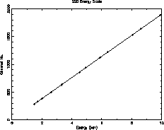
Figure 2: Energy scale of the Si(Li) solid state detector.
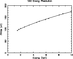
Figure 3: Resolution of the Si(Li) solid state detector.
The SSD energy scale has been characterized by measuring the
characteristic lines of a number of elements, and is shown in Figure
2. A quadratic fit to the data yields an energy scale of
approximately 5.25 eV per channel, given as  , where E is the energy in keV and C is the channel
number of the 2048-channel MCA.
, where E is the energy in keV and C is the channel
number of the 2048-channel MCA.
Spectral resolution of the SSD as a function of energy is presented in Figure 3, plotting FWHM(eV) vs. energy(keV). The data has been fitted with the standard function:

where N is the RMS noise in electrons,  is the energy needed
to create one electron-hole pair (3.76 eV/pair at 77K for Si(Li)), F
is the Fano factor and E is the photon energy in eV.[9] This
yielded an electronic noise contribution to the FWHM of 73 eV and a
Fano factor of 0.122, consistent with values reported in the
literature[10].
is the energy needed
to create one electron-hole pair (3.76 eV/pair at 77K for Si(Li)), F
is the Fano factor and E is the photon energy in eV.[9] This
yielded an electronic noise contribution to the FWHM of 73 eV and a
Fano factor of 0.122, consistent with values reported in the
literature[10].
As noted above, we have not yet completely characterized this detector system. For purposes of the analysis presented here, we have assumed no dead layer in the silicon, such that X-rays which penetrate the Be window and the two surface layers (contact and oxide) are assumed to be detected, since the transmission loss through 3.5 mm of Si is negligible for the energies of interest. The estimated attenuation of the Be window plus the Au/Pd contact layer is 5.2% at 4 keV and decreases smoothly to only 0.4% at 10 keV. This is the region where we intend to rely on the SSD as a calibration standard. At energies below 4 keV, the net attenuation increases to 14% at 2 keV and contains features due to both the L-edges of Pd and the M-edges of Au. In this region the SSD results will be compared to results from the PTB/BESSY calibration, which is our standard for low energies.
Of those X-rays detected, typically 90% or more appear in the main photopeak, with the remainder appearing primarily in the Si escape peak (for energies above the Si edge at 1.84 keV) and in the low energy tail (representing partial charge collection due to scattering losses at the crystal boundaries). Typical spectra for Si K lines (1.74 and 1.84 keV) and Mn K lines (5.89 and 6.49 keV) are shown below in Figures 6 and 9, respectively. Additional features may include lines due to fluorescing of the Al aperture and the Au/Pd contact layer.
Numerous papers describing the spectral response of Si(Li) detectors to X-rays in this regime have appeared in the literature. For example, the model presented by Scholze and Ulm[11] describes the response in the range 0.1 - 5 keV, and that presented by He et al.[12] covers the range 5 - 60 keV. These models allow fitting of the low energy tail features that accompany the Gaussian full-energy photopeak and the Si escape peak in the SSD response to mono-energetic radiation.
The Scholze-Ulm model assumes no inactive silicon layer and fits observed data for a windowless Si(Li) SSD to within 2%. It utilizes a modified HYPERMET function which includes an exponential tail feature due to partial charge deposition from hot (non-thermalized) electrons interacting with the contact layer, with an additional step threshold attributed to a partial reflection of the hot electrons moving from the silicon region to the contact layer. A second spectral feature is a flat shelf attributed to the transmission of primary (photo- and Auger) electrons from the contact layer to the Si, and to escape of electrons from the Si to the contact layer. Above 3 keV, the contribution of these features to the total count rate is under 10%. However, the contribution of the tail component can reach as high as 20 - 30 % near the Si absorption edge at 1.84 keV. The model presented by He et al. is similar but omits the step threshold component of the tail, which is less important at higher energies.
While we have not yet performed a full analysis of our calibration
data, we do expect that by fitting such models to our SSD data we can
obtain counting rates for our sources with an accuracy better than 3%
in the range 4 - 10 keV, where the SSD serves as our primary
calibration standard. Uncertainties in the window and contact layer
thicknesses are estimated to be of order 10% and are one of the main
sources of uncertainty in the detection efficiency calculations for
X-rays below  4 keV. Adding in photon noise (
 ) and
any systematic errors in our line fitting method, we estimate that the
total uncertainty in our Si(Li) detection efficiency calculations is
below 3% for energies above 4 keV, and no worse than 5% in the
region 2 - 4 keV.
) and
any systematic errors in our line fitting method, we estimate that the
total uncertainty in our Si(Li) detection efficiency calculations is
below 3% for energies above 4 keV, and no worse than 5% in the
region 2 - 4 keV.
Measurements below 4 keV, including the K lines of Si (1.74
keV) and P (2.01 keV) will be compared with CCD calibration values
obtained at the PTB - BESSY facility, which is our primary standard
below 4 keV. Results presented below are for relative ratios
of counting rates in the main Gaussian photopeak of selected lines
(CCD vs. SSD), and should be considered to be indicative of the final
detection efficiency values for the CCDs to the
lines of Si (1.74
keV) and P (2.01 keV) will be compared with CCD calibration values
obtained at the PTB - BESSY facility, which is our primary standard
below 4 keV. Results presented below are for relative ratios
of counting rates in the main Gaussian photopeak of selected lines
(CCD vs. SSD), and should be considered to be indicative of the final
detection efficiency values for the CCDs to the  % level.