Next: 2.3.1.2 Waveform generation Up: 2.3.1 CCD Chips Previous: 2.3.1 CCD Chips
Next: 2.3.1.2 Waveform generation
Up: 2.3.1 CCD Chips
Previous: 2.3.1 CCD Chips
The array operates as follows: when an image is focused onto the CCD, photons which penetrate the electrode structure generate electron-hole pairs in the underlying silicon substrate, and the signal charges are stored in the potential wells beneath the electrode structure (gates). After an appropriate image accumulation time, clock pulses are applied to the electrodes to shift the potential wells and their associated charges across the device. Rows of data are moved one-by-one in parallel to the output register with each parallel clock pulse cycle. Each row placed in the output register is then moved pixel-by-pixel to the output amplifier, where it passes as an analog signal to the signal processing chains. At the end of each pixel clock cycle, the charge measured at the node is uniquely identified with a pixel address. For incident light in the visible band, the charge magnitude is proportional to the illumination level at the pixel.
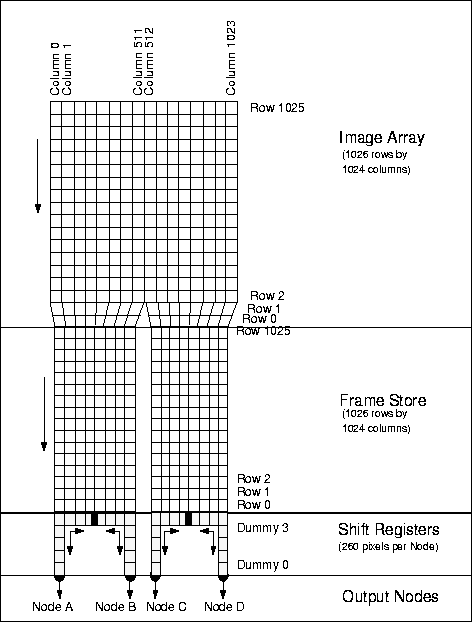
The electrodes are generally arranged in two groups; one group is fabricated over the top half of the array, and a second group over the bottom half. This latter half is shielded from light/X-rays, and is used to store successive image data frames previously collected in the top (labeled `image' in Fig. 2.10) section. This mode of operation is generally used for TV imaging and is called the framestore mode of operation. This eliminates the requirement for a mechanical shutter to shield the array during readout, since the data transfer from image to store section is accomplished in a fraction of the time (msecs) taken to read out the data in the array.
A visible light photon releases only one electron-hole pair, and consequently
many photons must be collected in each pixel for a measurable signal to be
produced. Therefore, at visible wavelengths CCDs are used as integrating
detectors, and typically the astronomical image exposures are several minutes
long. Conversely, a single X-ray photon has sufficient energy to form multiple
electron-hole pairs through the process of secondary ionization by the primary
photo-electron. An average of one electron-hole pair is liberated for each
3.65 eV of photon energy absorbed (this figure varies slightly with
temperature). The charge liberated by single X-ray photons
(![]() 100-1000 electrons) is easily detectable if the amplifier noise
is low enough. Therefore, at X-ray energies, CCDs can be used as photon
counting detectors, with the measured signal charges proportional to the
photon energies.
100-1000 electrons) is easily detectable if the amplifier noise
is low enough. Therefore, at X-ray energies, CCDs can be used as photon
counting detectors, with the measured signal charges proportional to the
photon energies.
This use as an imaging X-ray spectrometer requires that no more than one photon
is incident on each pixel in any image frame, which imposes a requirement that
image collection times be limited to ![]() seconds for typical astronomical
applications. In addition, the signal charge must ideally be completely
collected within the original pixel, transported to the output node without
losses due to imperfect charge transfer efficiency (CTE), and measured
without degradation by device readout noise.
seconds for typical astronomical
applications. In addition, the signal charge must ideally be completely
collected within the original pixel, transported to the output node without
losses due to imperfect charge transfer efficiency (CTE), and measured
without degradation by device readout noise.
Each of these requirements places special demands on the detector structure, and complicates the analysis of the data produced by the device. Charge collection efficiency is a function of the electric field strength at the site of X-ray absorption and is better in devices fabricated from higher resistivity material. Charge collection efficiency also improves as the pixel size increases. Even in high resistivity devices with large pixels, however, a significant fraction of all X-ray interactions will deposit charge in more than one pixel. A crucial consequence of imperfect charge collection is that not all detectable interactions yield useful spectroscopic information. Since the distribution of charge in a group of adjacent pixels is an indicator of the efficiency of charge collection, maximum spectral resolution can only be obtained if a multiplet of pixel values (usually a 3-pixel-by-3-pixel square neighborhood) is analyzed for each event. Moreover, one can trade spectral resolution for detection efficiency by varying event analysis parameters. (Analysis of pixel multiplets also provides a means to discriminate between X-ray photon events and background events produced by high-energy particles.)
Charge transfer within a CCD is subject to inefficiencies caused by the trapping of signal charge at discrete sites in the silicon. These may be at crystalline defects or at sites with a defect introduced by a manufacturing or design error. The probability of trapping any signal depends upon many factors such as the temperature, clock rate and previous history of charge passing through the trap. In ground-based optical imaging applications there is often sufficient signal in every pixel due to photons from the night sky background that all traps remain filled, and they have a negligible effect on the image data. For X-ray photon counting applications, there is no such background, and the event arrival rate requirements noted above almost guarantee that traps will de-populate between the arrival of successive signal packets. Charge transfer losses therefore tend to be more severe for X-ray astronomy. The result is that, even with a charge transfer inefficiency as low as 10-5 per pixel, charge packets traversing 1000 pixels will lose 1% of their signal, producing an apparent spatially varying gain function. In principle this is correctable, but the variation of the transfer losses with other parameters, particularly radiation damage, hinder this correction.
A particular case of concern arises when charge transfer is not
perfect, and a high photon flux strikes the CCD. In this case
charge will be removed from photon induced charge packets, but when
a second charge packet arrives some of the traps will still be filled.
The second photon thus experiences a different charge transfer efficiency
than the first. The output spectrum has poorer energy resolution
and the determination of the X-ray energy to charge packet size requires
a flux correction term. This problem has been termed `sacrificial
photons' by the MIT group, and detailed studies will be conducted
during ACIS calibration and beyond to assess the severity of the
problem. Tools to model the effect are described in Sec. 4.5.1,
page ![[*]](/images/LatexHtml/cross_ref_motif.gif) .
.
The X-ray energy required to liberate a charge pair in a semiconductor is approximately an order of magnitude lower than in gas detectors, hence the potential spectroscopic advantage of CCD detectors. In a silicon device, the FWHM energy resolution in eV is given by
| |
(1) |
Examination of equation 2.1
reveals that the CCD readout noise must be minimized
in order to exploit the potential for X-ray spectroscopy offered by the silicon
properties. Reducing read noise to ![]() 1 electron results in Fano noise
limited performance down to energies of 0.1 keV.
1 electron results in Fano noise
limited performance down to energies of 0.1 keV.
The X-ray energy is inferred from the size of charge packet collected in the CCD (Ne) by assuming proportionality,
| (2) |
A potentially larger effect at low energy results from incomplete charge collection in backside illuminated (BI) chips. Because low energy X-rays are absorbed very near to the first surface they strike, BI low energy interactions occur very near to the back surface. This surface has been subjected to potential crystal lattice damage in the process of removing the substrate material. Preliminary lab results suggest the possibility that charge from these low energy photons may be lost to these damage sites, resulting in non-linearity of the detected charge to the incident photon energy flux below one keV.
John Nousek