 Table of Contents
 Previous Chapter
Table of Contents
Previous Chapter
The purpose of the Timed Exposure PRAM Builder is to generate and load CCD-controller Program RAM instructions which clock the CCDs for the Timed Exposure Science Mode.
The following lists the uses of the Timed Exposure PRAM Builder:
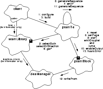
The following illustrates the relationships used by the Timed Exposure PRAM Builder class, PramTe, and a utility class which is used by the PRAM builder to manage PRAM Block output, PramBlock.
FIGURE 164. Timed Exposure PRAM Builder class relationships
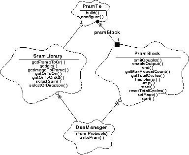
PramTe - This class is responsible for generating and loading a series of sequencer Program RAM words needed to clock a CCD for Timed Exposure mode. It provides a function which sets the desired clocking parameters (configure), and provides a function which generates and loads the clocking sequence into a particular DEA CCD-controller (build).
PramBlock - This class is responsible for emitting PRAM blocks to the DEA, each containing a header and one or more couplet entries. It is used by PRAM builders, such as PramTe and PramCc (see Section 35.0), to load entries into PRAM. It provides functions which reset the instance to the start of PRAM and disable output to the DEA (reset), start and end a PRAM block (start, end), cause jump to a new PRAM page (jump), start writing to a new page within PRAM (setPage), track the total number of clock cycles used by a block of PRAM (resetTotalCycles, getTotalCycles), emit a PRAM couplet (emitCouplet), obtain the maximum repeat cycles supported by a single couplet (getMaxRepeatCount), determine if an error was encountered while writing to the DEA (hasIoError), and enable output of PRAM words to the DEA (enableOutput).
DeaManager - This class is provided by the Protocols class category, and is responsible for managing access to the DEA interface. It provides a function which the builder uses to load words into a CCD-controller's Program RAM (writePram).
SramLibrary - This class is responsible for providing the PRAM builder with the Sequencer RAM (SRAM) locations of various primitives. It provides functions which select certain clocking options to use, such as the attenuated timing for the output register clocking, or the direction to clock the output registers (selectGain, selectOrDirection). It provides functions which supply the address of an SRAM block which does nothing (getIdle), which clock and sample 1 pixel from the output register to the output node (getOrToOn), clock and sum two pixels from the output register to the output node (getOrToOnX2). It also provides functions which return the starting SRAM block and number of contiguous blocks used to clock one row from the image array to the framestore (getImageToFrame), and which clock one row from the framestore into the output registers (getFrameToOr).
Figure 165 illustrates a graphical representation of a single CCD. The figure on the left of the illustration presents a simplified picture of the main CCD components, and the figure on the right illustrates the pixel dimensions of each of the components.
FIGURE 165. Graphical CCD Representation
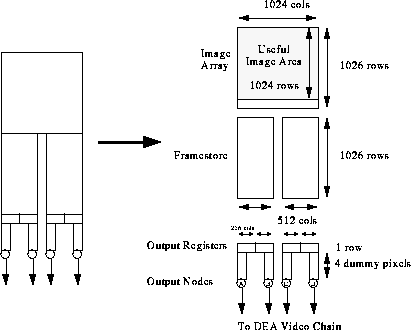
Each CCD consists of an Image Array, a Framestore, two output registers and four output nodes. Only 1024 of the 1026 Image Array rows are used for data acquisition.
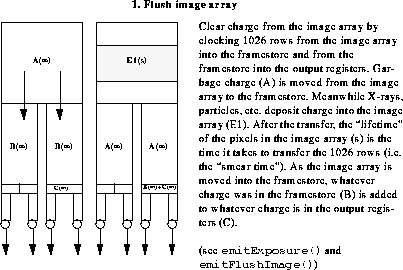
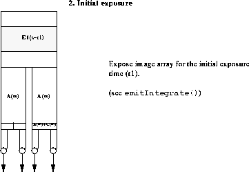
The following illustrates the sequence of operations used to clock CCDs in Timed Exposure Mode (NOTE: For a description of the used SRAM primitives, see Section 34.4.3. The PRAM builder function associated with the action is posted at the bottom of each description).:
SRAM consists of a collection of blocks, where each block performs a clocking operation. Some operations can be performed in a single SRAM block, whereas others, due to power constraints, require a series of SRAM blocks. Table 28 lists the SRAM operations used for Timed Exposure Clocking, where each SRAM block takes 1 pixel clock (~10�s) to execute.
 TABLE 28. Timed Exposure SRAM Operations
------------------------------------------------------------------------------------------------
Operation Number of Description
SRAM Blocks
This section describes the format of the PRAM words. PRAM consists of collections of word pairs known as `couplets.' Each couplet contains the address of one SRAM block to invoke, a repeat counter indicating the number of times to repeat the block, and a pixel code, which instructs the Front End Processors (FEPs) how to process pixels being clocked while the SRAM block is being invoked. Each invocation of a couplet takes 1 pixel clock period (~10�s).
While PRAM is running, pixel clocks are always being delivered to the FEPs, regardless of whether pixel data is being clocked out of the CCDs or not. The pixel code portion of the couplets indicate how the FEPs interpret the data. Valid pixel data is flagged using a "Valid Pixel" code, and overclock pixels are flagged using an "Overclock" code. All other codes cause the clocked pixel data to be ignored. These include the "Vsync" code, which indicates that a new image has been started, the "Hsync" code, which indicates that a new image row is about arrive, and the "Ignore" code, which indicates that the clocked pixel should be completely ignored by the FEPs.
Each collection of couplets is preceded by a pair of `header' words. The header consists of the number of couplets which follow the block, the number of times to repeat the collection of couplets, and an action to perform once the collection of couplets completes. These actions include: halt the sequencer, continue to the header immediately following the couplet collection, jump to the first PRAM location (restart), and jump to the indicated PRAM page.
The format of this header is as follows:
--------------------------------------------- 15 14 13 12 11 0--------------------------------------------- 1 1 Option PRAM Block Repeat Count 1 0 Page Jump Couplet Count ---------------------------------------------
------------------------------------------ 15 14 13 12 11 5 4 3 0------------------------------------------ 0 1 SRAM Page Address 0 PixCode 0 0 0 0 Major Cycle Count ------------------------------------------
PRAM Memory is organized around four contiguous pages, each containing 8192 words. The "jump" option of the PRAM Header causes PRAM to transfer control to the beginning of the specified page once the current PRAM block completes execution.
The following illustrates the clocking algorithm using pseudo-code, where the bolded text indicates operations which utilize the header repeat counter, italicized text indicates operations which can be accomplished using a single SRAM block and utilize the couplet repeat counter, and the underlined text indicates looping operations which are "unrolled" by the builder:
PRAM Page 0:
/* ---- Expose primary exposure time ---- */
IF primary exposure time is less than transfer time
Flush image array into framestore
ENDIF
Integrate CCD for (primary exposure time - transfer time)
/* ---- Transfer image to DPA ---- */
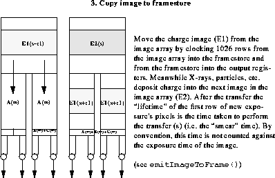
Move 1026 rows from the image array to the framestore
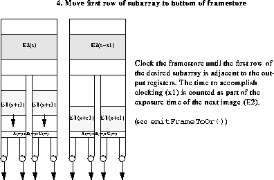
Locate first row of subarray to first row of framestore
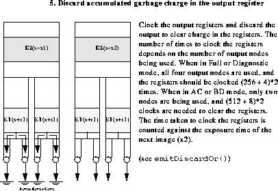
Discard output register
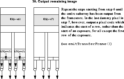
REPEAT for each subarray row
IF 2x2 sum
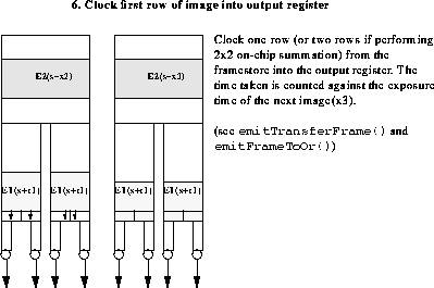
Move two rows from framestore to output registers
ELSE
Move one row from framestore to output registers
ENDIF
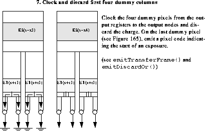
Discard 4 dummy output register pixels
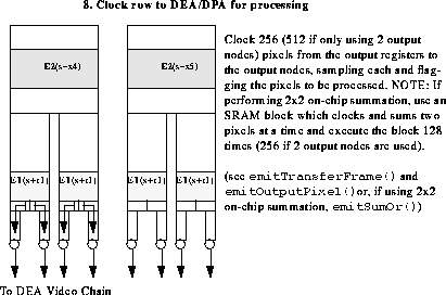
REPEAT for all pixels in output register
IF 2x2 sum
Clock, sum and sample 2 pixels from output registers
ELSE
Clock and sample 1 pixel from output registers
ENDIF
ENDREPEAT
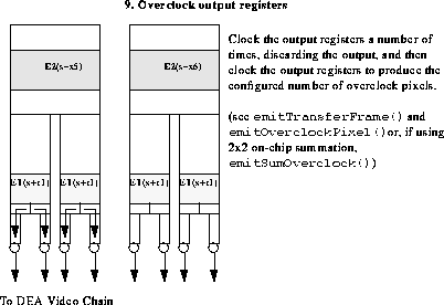
Discard output register pixels prior to producing overclocks
REPEAT for each overclock pixel
IF 2x2 sum
Clock, sum and sample 2 overclocks from output register
ELSE
Clock and sample 1 overclock pixel from output register
ENDIF
ENDREPEAT
ENDREPEAT
/* ---- Secondary exposures ---- */
REPEAT duty cycle times
/* --- Expose Secondary exposure time --- */
IF secondary exposure time is less than transfer time
Flush image array into framestore
ENDIF
Integrate CCD for (secondary exposure time - transfer time)
Transfer subarray image to DPA as described above
ENDREPEAT
Jump to PRAM Page 0
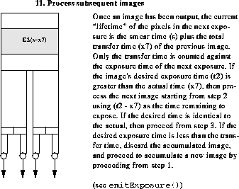
Due to constraints in the ability of the power-supply to deliver enough current to clock large numbers of pixels in all CCDs, each major set of contiguous row transfers from the image array to the framestore, or from the framestore to the output registers must be performed at different times on each CCD. In order to avoid noise from large row transfers on one CCD affecting the Analog-to-Digital conversion on another, all CCDs transfer their respective images to the DEA video system at the same time (NOTE: The time an image spends in the Framestore will be different for each CCD used in a single clocking sequence).
Figure 166 illustrates a one-and-a-half exposure time-line when clocking six CCDs.
FIGURE 166. Single CCD Clocking Sequence
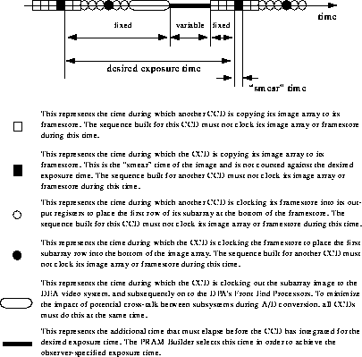
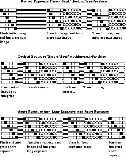
Figure 167 illustrates various clocking scenarios for CCDs in parallel.
FIGURE 167. Multiple CCD Clocking
In order to schedule each portion of the clocking operation, the PRAM builder must compute the time required to perform the image array to framestore transfer for a CCD, the time to position the first row of a subarray to the bottom of the framestore, and the time to transfer the subarray image to the DEA video system, and subsequently, on to the DPA's FEPs.
The time to transfer one row from the image array to the framestore is determined by the number of SRAM major cycles needed to perform the operation. The time to transfer the entire image array, is computed by multiplying the answer by 1026 rows. The minimum exposure time supported by the instrument is this result, multiplied by one less than the number of CCDs.
The time to position the subarray to the end of the framestore is the number of SRAM major cycles needed to clock 1 row in the framestore times the location of the first row (row 0) of the subarray (relative to CCD image row 0) plus 2 (to handle the two unused rows at the bottom of the image array).
The time taken to transfer the subarray image from the framestore to the DPA is a function of the number of rows in the subarray, the output node configuration, and the on-chip summing selection. In order to reduce the possibility of error when and if changes are made in how images are transferred from the framestore, the builder uses a two-pass approach when building images (see Section 34.5.2).
This section describes the design and use of the PramBlock class. This class is responsible for generating PRAM blocks (see Section 34.4.4), and loading these blocks into the DEA.
Figure 168 illustrates the overall behavior of the PramBlock class, in the form of a finite-state machine. The substates and transitions within the Output Disabled and Output Enabled superstates are identical, except that while in the Output Disabled state, the PramBlock class does not issue write requests to the DeaManager.
FIGURE 168. PramBlock Behavior
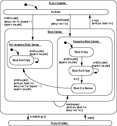
Clients use the PramBlock class to construct a series of non-repeating and repeating PRAM blocks. Since all useful PRAM loads within ACIS consist of an infinite loop, and since such loops require a page-jump, the client terminates the with a call to jump(), which forms the main infinite-loop of the PRAM sequence, and closes out the last PRAM block in the load.
For example, to build and emit a sequence on PRAM Page 0 which consists of a series of non-repeating blocks, followed by a block which repeats its contents 10 times, followed by a jump to the beginning of the page, the client issues the following call-sequence:
pramBlock.reset()
pramBlock.enableOutput()
pramBlock.setPage(0)
pramBlock.emitCouplet(...)
pramBlock.emitCouplet(...)
.
.
.
pramBlock.start(10)
pramBlock.emitCouplet(...)
pramBlock.emitCouplet(...)
.
.
.
pramBlock.end()
pramBlock.jump(0)
This produces a PRAM load which consists two PRAM blocks. When run, the first block will execute once and will then continue to the next adjacent block. The second will be executed 10 times, and once complete, will jump to the block at the start of PRAM Page 0 (which contains the first block).
In order to determine the total number of PRAM clock cycles used by a PRAM block, the client adds calls to resetTotalCycles() and getTotalCycles(). For example, the following determines the time it will take to execute the 2nd PRAM block, in terms of PRAM cycles:
pramBlock.reset()
pramBlock.enableOutput()
pramBlock.setPage(0)
pramBlock.emitCouplet(...)
pramBlock.emitCouplet(...)
.
.
pramBlock.resetTotalCycles()
pramBlock.start(10)
pramBlock.emitCouplet(...)
pramBlock.emitCouplet(...)
.
.
.
pramBlock.end()
pramBlock.getTotalCycles()
pramBlock.jump(0)
Figure 169 illustrates the use of the PramTe class to generate a PRAM load for Timed Exposure mode clocking (NOTE: The load call to sramLibrary, and loadSequencer call to deaManager are for reference information only. For more detail, see Section 36.0).
The PramTe builder uses a two-pass approach to constructing PRAM. The first pass is used to calculate the minimum integration time (in terms of clock cycles) which the current parameter set can support without an added flush of the image-array. The second pass is used to actually produce and store the generated sequence.
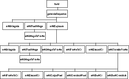
Figure 170 illustrates a structure chart, indicating the functional hierarchy within the PramTe class:
FIGURE 170. PramTe Class Internal Structure Chart
Hierarchy:
Superclasses:
none
Public Uses:
SramLibrary
Public Interface:
Operations:
PramTe()
build()
configure()
Protected Interface:
Operations:
emitDiscardOr()
emitExposure()
emitFlushImage()
emitFrameToOr()
emitImageToFrame()
emitIntegrate()
emitOutputPixel()
emitOverclockPixel()
emitSumOr()
emitSumOverclock()
emitTransferFrame()
generateSequence()
Implementation:
Has-A Relationships:
PramTe
PramTe
Boolean
Arguments:
CcdId ccdId
unsigned phaseslot
Documentation:
This function builds a PRAM sequence and loads the sequence into the DEA CCD-controller specified by ccdId. phaseSlot specifies the parallel transfer slot used by the CCD. phaseSlot can range from 0 to one minus the number of configured CCDs (see configure()). The function returns BoolTrue if the sequence is successfully built and loaded into the DEA. It returns BoolFalse if an error was encountered while trying to write to the DEA.
PramTe
Boolean
Arguments:
unsigned boardcnt
unsigned expPrimary
unsigned expSecondary
unsigned expDuty
unsigned rowstart
unsigned rowend
Boolean sum2x2
QuadMode quadrants
unsigned ocPairs
Boolean attenuate
const SramLibrary& sramlib
Documentation:
This function configures the Timed Exposure PRAM builder. boardcnt is the total number of CCDs being clocked, expPrimary is the primary exposure time, expSecondary is the secondary exposure time, and expDuty is the number of expSecondary exposures per expPrimary exposures. rowstart is the index of the first CCD row of the subarray, and rowend is the index of the last row. sum2x2 indicates whether or not to perform 2x2 on-chip summation. quadrants indicates the output node configuration and clocking direction (Full, Diagnostic, AC, or BD). ocPairs indicates the number of pairs of overclock pixels to generate. attenuate indicates whether or not to use 4:1 SRAM video timing. sramlib is a reference to the SRAM library to use for the run.
PramTe
void
Arguments:
unsigned npix
PramPixCode pixcode
Documentation:
Emit PRAM couplets which clock npix columns from the output register into the output node, each time, discharging the output node, effectively discarding the pixels. pixcode indicates the pixel code to use when discarding the pixels.
PramTe
unsigned
Arguments:
unsigned expclocks
Documentation:
Emit PRAM instructions to integrate the CCD for a period of time, and then transfer the exposed image to the DPA. The total integration of the image is specified by expclocks. This function returns the number of clock cycles taken to clock the image from the Framestore to the DPA (i.e. the minimum integration time that can be supported without a flush of the image-array).
PramTe
void
Arguments:
unsigned nrows
Documentation:
Emit PRAM instructions to transfer nrows rows from the image array to framestore and from the framestore to the output register for discard. This function calls emitImageToFrame() to emit the instructions for the transfer.
PramTe
void
Arguments:
unsigned nrows
Documentation:
Emit PRAM couplets which transfer nrows from the framestore into the output register. The charge from the rows will be summed together and with whatever charge exists in the output register.
PramTe
void
Arguments:
unsigned nrows
Documentation:
Emits PRAM directives to transfer nrows from the image array to the framestore and from the framestore to the output register.The charge from the framestore rows will be summed together with whatever charge exists in the output register.
PramTe
void
Arguments:
unsigned expcounts
Documentation:
This function emits an SRAM block which lets the CCD sit still (expose) for expcounts pixel clock cycles. (NOTE: If expcounts is 0, then no action is taken and the function immediately returns).
PramTe
void
Arguments:
unsigned npix
Documentation:
Emit PRAM couplets which transfer npix pixels from the output register to the output node and sample each pixel at the output node. This function calls sramLibrary>getOrToOn() to obtain the index of the SRAM block to use to output and sample a single pixel, and then calls pramBlock.emitCouplet(), passing npix as the repeat count, and using the PIXCODE_PIXEL pixel code to indicate to the DPA that the pixel is part of the image data.
PramTe
void
Arguments:
unsigned npix
Documentation:
Emit PRAM instructions to clock and sample npix overclock pixels from the output register. This function calls sramLibrary>getOrToOn() to obtain the index of the SRAM block to use to output and sample a single pixel, and then calls pramBlock.emitCouplet(), passing npix as the repeat count, and using the PIXCODE_OVERCLOCK pixel code to indicate to the DPA that the pixel is part of the image's overclock data.
PramTe
void
Arguments:
unsigned npix
Documentation:
Emit PRAM instructions to clock and sum two pixels from the output register into the output node, and then sample and transmit the result to the DPA. npix indicates the number of pairs of pixels to clock. This function calls sramLibrary>getOrToOnX2() to obtain the index of the SRAM block to use to sum and sample two pixels at a time, and then calls pramBlock.emitCouplet(), passing npix as the repeat count, and using the PIXCODE_PIXEL pixel code to indicate to the DPA that the pixel is part of the image data.
PramTe
void
Arguments:
unsigned npix
Documentation:
Emit PRAM instructions to clock and sum pairs of overclock pixels from the output register. npix indicates the number of pairs of overclock pixels to clock. This function calls sramLibrary>getOrToOnX2() to obtain the index of the SRAM block to use to sum and sample two pixels, and then calls pramBlock.emitCouplet(), passing npix as the repeat count, and using the PIXCODE_OVERCLOCK pixel code to indicate to the DPA that the pixel is part of the image's overclock data.
PramTe
void
Arguments:
unsigned nrows
Documentation:
Emit PRAM instructions to transfer nrows of an image from the framestore to the DEA/DPA via the output registers and output node.
PramTe
void
Arguments:
Boolean timingRun
Documentation:
This function runs through the PRAM generation process. If timingRun is BoolTrue, then the function computes and stores the minimum un-flushed integration time, into xfrTime, otherwise, xfrTime is not modified. Upon returning, xfrTime contains the transfer time for an exposure.
Hierarchy:
Superclasses:
none
Implementation Uses:
DeaManager
Public Interface:
Operations:
PramBlock()
emitCouplet()
enableOutput()
end()
getMaxRepeatCount()
getTotalCycles()
hasIoError()
jump()
reset()
resetTotalCycles()
setPage()
start()
Protected Interface:
Operations:
buildCouplet()
buildHeader()
emitHeader()
Private Interface:
Has-A Relationships:
PramBlock
PramBlock
void
Arguments:
unsigned sramaddr
PramPixCode pixcode
unsigned repeat
unsigned short[2] couplet
Documentation:
This function formats a PRAM couplet word pair, storing the formatted words into couplet. sramaddr is the SRAM block address to invoke, pixcode is the pixel code to emit during execution of the block and repeat is the number of times to repeat the block.
PramBlock
void
Arguments:
PramOp operation
PramPage page
unsigned couplets
unsigned repeat
unsigned short[2] header
Documentation:
This function formats a PRAM block header and stores the formatted words in header. operation is the action to take once the PRAM couplets have been processed and page is the PRAM page to jump to if operation specifies a jump. couplets is the total number of couplets in the block, and repeat is the number of times to repeat the block.
PramBlock
void
Arguments:
unsigned sramaddr
PramPixCode pixcode
unsigned repeat
Documentation:
This function builds a couplet word pair and writes the pair into the DEA's PRAM. sramaddr is the SRAM address of the SRAM block to invoke for the couplet. pixcode is the pixel code to associate with the pixels produced while the block is being invoked. repeat is the number of times to repeat the block.
PramBlock
void
Arguments:
PramOp operation
PramPage page
Documentation:
This function writes the block header to PRAM. operation is the action to take once the block has been executed, and page specifies which page to jump to if the operation warrants it.
PramBlock
void
Arguments:
CcdId ccd
Documentation:
This function enables output to the CCD indicated by ccd. To disable output, call reset().
PramBlock
void
PramBlock
unsigned
PramBlock
unsigned
PramBlock
Boolean
PramBlock
void
Arguments:
PramPage page
Documentation:
This function writes the header to the current block, issuing a jump operation to the PRAM page indicated by page.
PramBlock
void
PramBlock
void
PramBlock
void
Arguments:
PramPage page
Documentation:
This function sets the current PRAM address to the location corresponding to page.
PramBlock
void
Arguments:
unsigned repeat
Documentation:
This function flushes any previous block, and opens a new block at the current PRAM address. The opened block is configured to be executed repeat times.
 Next Chapter