 Table of Contents
 Previous Chapter
Table of Contents
Previous Chapter
The purpose of the Continuous Clocking PRAM Builder is to generate and load CCD-controller Program RAM instructions which clock the CCDs for the Continuous Clocking Science Mode.
The following lists the uses of the Continuous Clocking PRAM Builder:
The following illustrates the relationships used by the Continuous Clocking PRAM Builder class, PramCc. A detailed description of the PramBlock class is provided in Section 34.0.
FIGURE 171. Continuous Clocking PRAM Builder class relationships
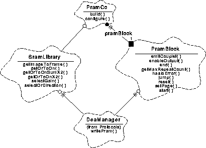
PramCc - This class is responsible for generating and loading a series of sequencer Program RAM (PRAM) words needed to clock a CCD for Continuous Clocking mode. It provides a function which sets the desired clocking parameters (configure), and provides a function which generates and loads the clocking sequence into a particular DEA CCD-controller (build).
PramBlock - This class is responsible for emitting PRAM blocks to the DEA, each containing a header and one or more couplet entries. It is used by PRAM builders, such as PramTe (see Section 34.0) and PramCc, to load entries into PRAM. It provides functions which reset the instance to the start of PRAM and disable output to the DEA (reset), start and end a PRAM block (start, end), cause jump to a new PRAM page (jump), start writing to a new page within PRAM (setPage), emit a PRAM couplet (emitCouplet), obtain the maximum repeat cycles supported by a single couplet (getMaxRepeatCount), determine if an error was encountered while writing to the DEA (hasIoError), and enable output of PRAM words to the DEA (enableOutput). A complete description of this class is provided with the description of the Timed Exposure PRAM Builder classes in Section 34.0
DeaManager - This class is provided by the Protocols class category, and is responsible for managing access to the DEA interface. It provides a function which the builder uses to load words into a CCD-controller's Program RAM (writePram).
SramLibrary - This class is responsible for providing the PRAM builder with the Sequencer RAM (SRAM) locations of various primitives (NOTE: The function names abbreviate "output register" as "Or" and output node as "On"). It provides functions which select certain clocking options to use, such as the attenuated timing for the output register clocking, or the direction to clock the output registers (selectGain, selectOrDirection). It provides functions which supply the address of an SRAM block which clock and sample 1 pixel from the output register to the output node (getOrToOn), clock and sum two pixels from the output register to the output node (getOrToOnX2), clock and sum, without sampling, two pixels into the output register (getOrToOnSumX2). It also provides a function which returns the starting SRAM block and number of contiguous blocks used to clock one row from the image array to the framestore and from the framestore to the output registers (getImageToFrame).
Figure 172 illustrates a graphical representation of a single CCD. The figure on the left of the illustration presents a simplified picture of the main CCD components, and the figure on the right illustrates the pixel dimensions of each of the components.
FIGURE 172. Graphical CCD Representation
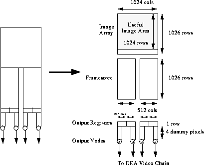
Each CCD consists of an Image Array, a Framestore, two output registers and four output nodes. Only 1024 of the 1026 Image Array rows are used for data acquisition.
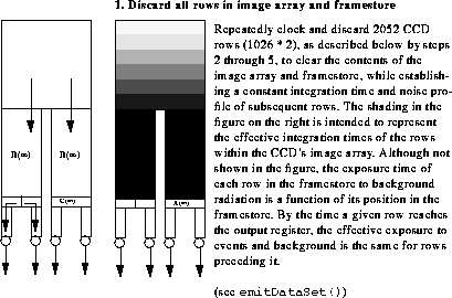
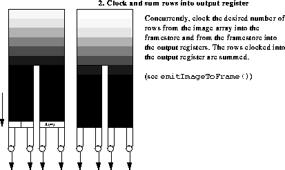
The following illustrates the sequence of operations used to clock out one summed CCD row in Continuous Clocking Mode (NOTE: For a description of the used SRAM primitives, see Section 35.4.3. The PRAM builder function associated with the action is posted at the bottom of each description):
SRAM consists of a collection of blocks, where each block performs a clocking operation. Some operations can be performed in a single SRAM block, whereas others, due to power constraints, require a series of SRAM blocks. Table 29 lists the SRAM operations used for Continuous Clocking Mode, where each SRAM block takes 1 pixel clock (~10�s) to execute.
 TABLE 29. Continuous Clocking SRAM Operations
-----------------------------------------------------------------------------------------------
Operation Number of Description
SRAM Blocks
This section describes the format of the PRAM words. PRAM consists of collections of word pairs known as `couplets.' Each couplet contains the address of one SRAM block to invoke, a repeat counter indicating the number of times to repeat the block, and a pixel code, which instructs the Front End Processors (FEPs) how to process pixels being clocked while the SRAM block is being invoked. Each invocation of a couplet takes one pixel clock period (~10�s).
While PRAM is running, pixel clocks are always being delivered to the FEPs, regardless of whether pixel data is being clocked out of the CCDs or not. The pixel code portion of the couplets indicate how the FEPs interpret the data. Valid pixel data is flagged using a "Valid Pixel" code, and overclock pixels are flagged using an "Overclock" code. All other codes cause the clocked pixel data to be ignored. These include the "Vsync" code, which indicates that a new image has been started, the "Hsync" code, which indicates that a new image row is about arrive, and the "Ignore" code, which indicates that the clocked pixel should be completely ignored by the FEPs.
Each collection of couplets is preceded by a pair of `header' words. The header consists of the number of couplets which follow the block, the number of times to repeat the collection of couplets, and an action to perform once the collection of couplets. These actions include: halt the sequencer, continue to the header immediately following the couplet collection, jump to the first PRAM location (restart), and jump to the indicated PRAM page.
The format of this header is as follows:
--------------------------------------------- 15 14 13 12 11 0--------------------------------------------- 1 1 Option PRAM Block Repeat Count 1 0 Page Jump Couplet Count ---------------------------------------------
------------------------------------------ 15 14 13 12 11 5 4 3 0------------------------------------------ 0 1 SRAM Page Address 0 PixCode 0 0 0 0 Major Cycle Count ------------------------------------------
PRAM Memory is organized around four contiguous pages, each containing 8192 words. The "jump" option of the PRAM Header causes PRAM to transfer control to the beginning of the specified page once the current PRAM block completes execution.
The following illustrates the clocking algorithm using pseudo-code, where the bolded text indicates operations which utilize the header repeat counter, italicized text indicates operations which can be accomplished using a single SRAM block and utilize the couplet repeat counter, and the underlined text indicates looping operations which are "unrolled" by the builder:
PRAM Page 0:
/* ---- Clock and emit first row of data set ---- */
Clock image array/framestore to sum "n" rows in output registers
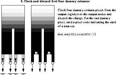
Discard 4 dummy pixels, and indicate start of data set (VSYNC)
REPEAT for all summed pixels in output register
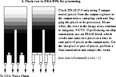
Clock output register to sum "m" pixels. Sample result.
ENDREPEAT
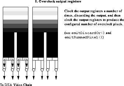
Discard output register pixels prior to producing overclocks
REPEAT for each overclock pixel sum
Clock output register to sum "m" overclocks. Sample result.
ENDREPEAT
Indicate end of row (HSYNC)
/* ---- Clock remaining rows of data set ---- */
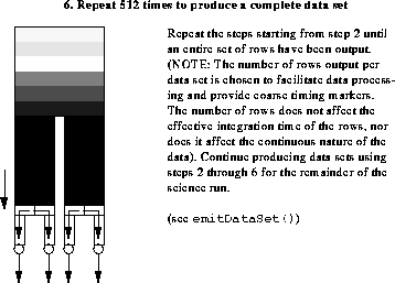
REPEAT for 511 rows
Clock image array/framestore to sum "n" rows in output registers
Discard dummy pixels
REPEAT for all summed pixels in output register
Clock output register to sum "m" pixels. Sample result.
ENDREPEAT
Discard output register pixels prior to producing overclocks
REPEAT for each overclock pixel sum
Clock output register to sum "m" overclocks. Sample result.
ENDREPEAT
Indicate end of row (HSYNC)
ENDREPEAT
Jump to PRAM Page 0
Assuming constraints on the maximum number of rows and columns that may be summed, phase-delays between image array/framestore row transfers on different CCDs, such as those used by Timed Exposure Mode (see Section 34.4.6), are not required.
Figure 173 illustrates the use of the PramCc class to generate a PRAM load for Continuous Clocking mode (NOTE: The load call to sramLibrary, and loadSequencers call to deaManager are for reference information only. For more detail, see Section 36.0). For a description of the use of the PramBlock class, see Section 34.5.1
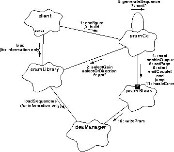
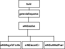
Figure 174 illustrates a structure chart, indicating the functional hierarchy within the PramTe class:
FIGURE 174. PramCc Class Internal Structure Chart
Hierarchy:
Superclasses:
none
Public Uses:
SramLibrary
Public Interface:
Operations:
PramCc()
build()
configure()
Protected Interface:
Operations:
emitDataSet()
emitDiscardOr()
emitImageToFrame()
emitSummedPixel()
generateSequence()
Private Interface:
Has-A Relationships:
Arguments:
CcdId ccdId
Documentation:
This function builds a PRAM sequence and loads the sequence into the DEA CCD-controller specified by ccdId. The function returns BoolTrue if the sequence is successfully built and loaded into the DEA. It returns BoolFalse if an error was encountered while trying to write to the DEA.
Arguments:
unsigned rowsum
unsigned colsum
QuadMode quadrants
unsigned ocPairs
Boolean attenuate
SramLibrary& sramlib
Documentation:
This function configures the Continuous Clocking PRAM builder. rowsum is the number of rows to sum, and colsum is the number of columns to sum per output pixel. quadrants indicates the output node configuration and clocking direction (Full, Diagnostic, AC, or BD). ocPairs indicates the number of pairs of overclock pixels to generate. attenuate selects the SRAM timing. If BoolFalse, use 1 electron/ADU timing, and if BoolTrue, use timing which produces 4 electrons/ADU.sramlib is a reference to the SRAM library to use when building PRAM.
Arguments:
unsigned nrows
Boolean flush
Documentation:
Emit PRAM instructions to produce 1 data set of continuously clocked CCD pixels. nrows specifies the number of rows to emit in the data set, and flush indicates whether or not to use the produced data set. If flush is BoolFalse, treat clocked data as valid pixels. If flush is BoolTrue, then ignore all clocked data. This is used to discard the initial contents of the image array and framestore at the start of the run.
Arguments:
unsigned npix
unsigned pixcode
Documentation:
Emit PRAM couplets which clock npix columns from the output register into the output node, each time, discharging the output node, effectively discarding the pixels. pixcode indicates the pixel code to use when discarding the pixels.
Arguments:
unsigned nrows
Documentation:
This function clocks nrows from the image array to the framestore, and from the framestore into the output register. The rows clocked into the output register are summed with each other, and with charge already in the output registers.
Arguments:
unsigned npix
PRAM_PIXCODE pixcode
Documentation:
Emit PRAM couplets which emit a series of npix summed pixels from the output register. Each output pixel is flagged with the pixcode pixel code, and consists of the sum of colSum output register pixels.
 Next Chapter