 Table of Contents
 Previous Chapter
Table of Contents
Previous Chapter
This section describes the main interfaces used by the ACIS Science Instrument Software.
The Mongoose Microcontroller is based on an R3000 processor. The following sections provide a brief overview the R3000 Core Processor. This information is taken from "MIPS RISC Architecture," by Kane, published by Prentice Hall, and from "The MIPS Programmer's Handbook," by Farquhar and Bunce, published by Morgan Kaufmann. A description of the Mongoose extensions to the R3000 is provided in Section 4.2 .
This section provides a brief overview of some aspects of the R3000 instruction set. The R3000 is a reduced-instruction-set-computer (RISC) and has a reasonably small instruction set. Each processor instruction occupies 1 32-bit word, and, barring memory waits, is effectively executed in 1 machine cycle. Certain instructions, however, require the compiler, assembler or software engineer to be careful in the ordering of instructions. For example, memory load instructions prohibit the instruction immediately following it from using the fetched value, and conditional and unconditional branch instructions always execute the instruction immediately following the branch instruction, regardless of whether the branch is taken or not.
The R3000 assemblers are "smart" in that they provide enhanced instructions, and make code-generation decisions when possible. For example, most of the assemblers provide a "Load Constant Address" instruction which the assembler may translate into one or two core instructions depending on the nature of the address. If the address has non zero values in both the upper and lower 16-bits, the assembler will produce a "lui" to load the upper 16-bits, followed by a "ori" to add in the lower 16-bit of the address. If the lower 16-bits are zero, the assembler will omit the "ori" operation. If the upper 16-bits are zero, the assembler will just use a "li" instruction to load the lower 16-bits and zero the upper 16.
The following is a list of the core R3000 instructions provided by the processor:
 TABLE 4. R3000 Core Instruction Set
------------------------------------------------------- Mnemonic Instruction------------------------------------------------------- Arithmetic Instructions add Add addi Add Immediate (16-bit) addiu Add Unsigned Immediate addu Add Unsigned and AND andi AND Immediate div Divide divu Divide Unsigned mult Multiply multu Multiply Unsigned nor NOR or OR ori OR Immediate sll Shift Logical Left sllv Shift Logical Left Variable sra Shift Right Arithmetic srav Shift Right Arithmetic Variable srl Shift Logical Right srlv Shift Logical Right Variable sub Subtract subu Subtract Unsigned xor XOR xori XOR Immediate Branch and Jump Instructions bczf Branch Co-processor Z Flag False bczt Branch Co-processor Z Flag True beq Branch if Registers Equal bgez Branch if register >= 0 bgezal Branch and Link if register >= 0 bgtz Branch register > 0 blez Branch register <= 0 bltz Branch register < 0 bltzal Branch and Link register < 0 bne Branch if registers not equal j Jump jal Jump and Link jlr Jump and Link Register jr Jump Register Co-processor Instructions cfcz Move from Co-processor Z Control Register copz Co-processor Z Operation ctcz Move to Co-processor Z Control Register lwcz Load Word to Co-processor Z Register mfc0 Move from System Co-processor Register mfcz Move from Co-processor Z Register mtc0 Move to System Co-processor Register mtcz Move to Co-processor Z Register tlbp System Co-processor Probe TLB for Match tlbr System Co-processor Read Indexed TLB Entry tlbwi System Co-processor Write Indexed TLB Entry tlbwr System Co-processor Write Random TLB Entry rfe System Co-processor Return from Exception swcz Store Word from Co-processor Z Register Load and Store Instructions lb Load byte lbu Load byte unsigned lh Load half-word lhu Load half-word unsigned lui Load Upper 16-bits immediate lw Load Word lwl Unaligned Load Word Left lwr Unaligned Load Word Right mfhi Move to High Accumulator (mult,div) mflo Move from Low Accumulator mthi Move to High Accumulator mtlo Move to Low Accumulator sb Store Byte sh Store Half-word sw Store Word swl Unaligned Store Word Left swr Unaligned Store Word Right Miscellaneous Instructions break Breakpoint slt Set on Less Than slti Set on Less Than Immediate sltiu Set on Less Than Immediate Unsigned sltu Set on Less Than Unsigned syscall System Call -------------------------------------------------------
This section provides an overview of the R3000's System Co-processor (CU0). This co-processor's registers can be read via the "mfc0" CPU instruction, and written to via the "mtc0" CPU instruction. This co-processor provides the following registers:
This section describes the R3000 System Co-processor's Status Register. The following lists the bit fields contained within this register:
-------------------------------------------------------------------------------------------- 31 28 27 23 22 21 20 19 18 17 16 15 8 7 6 5 4 3 2 1 0-------------------------------------------------------------------------------------------- CU 0 BEV TS PE CM PZ SwC IsC IntMask 0 KUo IEo KUp IEp KUc IEc --------------------------------------------------------------------------------------------
IEc, IEp, IEoKUc, KUp, KUoIntMaskIsCSwCPZCMPETSBEVCU (0-3)
-------------------------------------------- 15 14 13 12 11 10 9 8-------------------------------------------- INT6 INT5 INT4 INT3 INT2 INT1 Sw2 Sw1 --------------------------------------------
SwINT
------------------ 31 30 29 28------------------ CU3 CU2 CU1 CU0 ------------------
CU0CU1CU2CU3Interrupt Enable BitsKernel/User Mode BitsInterrupt MaskBootstrap Exception VectorsCo-processor Usable BitsThis section describes the R3000 System Co-processor's Interrupt Cause Register.
-------------------------------------------------------------- 31 30 29 28 27 16 15 10 9 8 7 6 5 2 1 0-------------------------------------------------------------- BD 0 CE 0 IP[5..0] Sw 0 ExcCode 0 --------------------------------------------------------------
ExcCodeSwIP[5..0]CEBDExcCodeTABLE 5. Cause Register Exception Code Values
------------------------------------------------------------- Code Cause------------------------------------------------------------- 0 - Int: External Interrupt (including Mongoose CSI) 1 - MOD: TLB Modification exception (not on Mongoose) 2 - TLBL: Load or fetch TLB miss exception (not on Mongoose) 3 - TLBS: Store TLB miss exception (not on Mongoose) 4 - AdEL: Load or fetch Address Error Exception 5 - AdES: Store Address Error Exception 6 - IBE: Instruction Bus Exception 7 - DBE: Data Bus Exception 8 - Sys: SysCall Exception 9 - Bp: Breakpoint Exception 10 - RI: Reserved Instruction Exception 11 - CpU: Co-processor Unusable Exception 12 - Ovf: Arithmetic Overflow Exception 13-15: Reserved -------------------------------------------------------------
Sw[0,1]IP[0..5]CE[0..1]BDThis section describes the R3000 System Co-processor's Exception Program Counter Register. This register contains the address to resume after processing an interrupt or exception. Typical code for ending an exception is as follows:
mfc0    k0,C0_EPC      # Get return address into kernel register 0
nop          # 1 instruction delay after a mfc0 before value valid
jr  k0        # Jump to resumption address
rfe          # Use delay slot to tell CU0 to restore flags
This section describes the R3000 System Co-processor's Bad Virtual Address Register. This register contains the virtual address which caused an address exception. This register is not used for bus errors.
The following sections provide a brief overview of the Mongoose Microcontroller registers. This information is taken from "Mongoose ASIC Microcontroller Programming Guide, September 1993," by Brian Smith, NASA Reference Publication 1319.
This section describes the Mongoose Microboot Control Word. This word is located in the last location in Boot ROM (or RAM in the case of the FEPs) and is used by the Mongoose during hardware initialization (prior to any software activity) to configure its Instruction and Data cache memory chip layout. The format of this register is as follows:
------------------------------------------------- 31 8 7 5 4 3 2 1 0------------------------------------------------- Unused Mux. Decode I-cache D-cache Unused -------------------------------------------------
D-cacheI-cacheMux. DecodeThis section provides an overview of the Mongoose Command and Status interface registers. The Mongoose Microcontroller provides a block of command and status interface registers, located at address 0xb4c00000. This block contains the following registers:
The following illustrates the memory layout for this block of registers:
Extended Interrupt Mask  0xbf400000
Extended Interrupt Cause  0xbf400004
Configuration Register  0xbf400008
DMA Origin  0xbf40000c
DMA Destination  0xbf400010
DMA Word Count  0xbf400014
Watchdog Count  0xbf400018
Timer Count  0xbf40001c
Uart Command/Status  0xbf400024
Uart Data  0xbf400028
I-cache Address  0xbf40002c
I-cache Data  0xbf400030
This section describes the Mongoose Configuration Register. This register is used to enable/disable the general purpose timer, to initiate memory transfers using the DMA Controller, and to select the number of memory wait-states to use in external, uncached memory. The format of the configuration register is as follows:
----------------------------------------------------------------------- 31 30 29 28 27 26 25 21 20 17 16 0----------------------------------------------------------------------- Unused Timer Enable Unused DMA Type Unused Wait State Unused -----------------------------------------------------------------------
Wait StateDMA TypeTimer EnableThis section describes the Mongoose's Instruction Cache access registers and the procedure used to read and write the contents of the Instruction Cache. The Mongoose Instruction cache is loaded and dumped using an address and data register. The format of the Mongoose Instruction Cache Address register is as follows:
----------------------------------------------------- 31 30 29 20 19 2 1 0----------------------------------------------------- R W 0 Instruction Address Bits 2:19 0 -----------------------------------------------------
Instruction AddressWRTo write into the instruction cache, clear the bits 0, 1 and 20 through 31 of the destination address, OR a 1 into the Write-to-Icache control bit, write the desired data word to the data register, wait at least one CPU cycle, then write the formatted address to the Instruction Cache address register.
To read a word, zero bits 0, 1 and 20 through 31 of the source address, OR a 1 into the Read-command bit, write the formatted address into the Instruction Cache address register, wait at least one CPU cycle, and then read the Instruction Cache data register.
This section describes the Mongoose Extended Interrupts. The Mongoose supports a set of extended interrupts and exceptions, which when asserted and unmasked, cause INT3 (IP[2]) to be asserted on the R3000 Core (see Section 4.1.2.1 and Section 4.1.2.2 ). The set of interrupts and exceptions include:
This section describes the Mongoose Extended Interrupt Mask Register. This register is used to prevent one or more of the extended interrupt sources from causing an interrupt. A `1' in the mask allows interrupts from the corresponding source, and a `0' prevents the source from interrupting the processor. The format of the extended mask register is as follows:
---------------------------------------------------------------------------------------------------- 31 16 15 14 13 12 11 10 9 8 7 6 5 4 3 2 0---------------------------------------------------------------------------------------------------- Unused Watchdog Timer DMA Rx Tx MemE InsBE DataBE DmaBE WBE Int3a Int3b Int3c Unused ----------------------------------------------------------------------------------------------------
Int3cInt3bInt3aWBEDmaBEDataBEInsBEMemETxRxDMATimerWatchdogThis section describes the Mongoose Extended Cause Register. When read, this register returns the list of sources which have requested interrupt service. A `1' indicates that the corresponding device has asserted an interrupt request. A `0' indicates that no interrupt request is pending from the device. When written to, this register clears the pending request. The format for this register is identical to that for the Extended Mask Register (see Section 4.2.5.1 ).
This section describes the Mongoose DMA Controller. The Mongoose DMA Controller is configured using the DMA Controller Starting Origin Register, DMA Controller Starting Destination Register, the DMA Controller Count Register, and the DMA Type bits in the Mongoose Configuration Register (see Section 4.2.3 ).
This section describes the Mongoose Watchdog Timer. The Watchdog Timer's time-out duration is established by writing a value into its Count Register. Upon reset, the counter's value is 0xffffffff. This count register decrements with each CPU cycle (10MHz). When the count reaches 0, the timer generates a hardware pulse, which on ACIS, is connected to the processor's reset logic.
This section describes the Mongoose General Purpose Timer. The General Purpose Timer's time-out duration is established by writing a value into its Count Register. Upon reset, the counter's value is 0xffffffff, and the timer is disabled. When enabled via the Configuration Register (see Section 4.2.3 ), this count register decrements with each CPU cycle (10MHz). When the count reaches 0, the timer asserts the Timer End of Count extended interrupt (see Section 4.2.5 ), and the counter wraps to 0xffffffff and continues to decrement with each CPU cycle.
The following sections describe the Back End Processor hardware interfaces. This information is taken from the "DPA Hardware Specification and System Description, Rev. 04," by Dorothy Gordon, MIT Drawing Number 36-02104. Additional information is included in advance of future publications of this document, and is marked as TBD.
This section illustrates the overall Back End Processor hardware memory map:
TABLE 6. Back End Processor Memory Map Overview
----------------------------------------------------------------------------------------- Virtual Byte Size Name Use Address----------------------------------------------------------------------------------------- 0xbfc00000 0x8000 Boot ROM Contains Bootstrap loader software (see Section 13.0 ) and Microboot Control Word (see Section 4.2.1 ) 0xbf800000 N/A External Debug Board Debug board used for development/pre- flight testing 0xbf400000 0x30 Mongoose CSI Subblock see Section 4.2 0xb8000000 0x100000 Flight ROM Contains the delivered image of the instrument software code and initialized data. This image is copied into I-cache and D-cache by the Bootstrap loader soft ware. 0xa8000000 0x7ff0000 FEP Shared Memory Shared FEP RAM used for mailboxes, Addresses ring-buffers, and bias maps and bias par ity planes. 0xa0180000 N/A BEP I/O Devices see below 0xa0000000 1 MB Bulk Memory and FEP BEP-populated RAM used for telemetry Shared Memory buffers. Addresses 0x80080000 0x80000 Instruction Cache Contains copy of patched and running (SEU-immune) code. Since this RAM can only be written to via the Mongoose CSI (see Section 4.2.4 ), portions of this area are used to preserve patch lists, system configuration parame ters, science parameter blocks, and DEA parameter blocks across resets. 0x80000000 0x20000 Data Cache Contains copy of patched initialized data. (SEU-immune) Used for run-time stacks, RTX resources, and program data. -----------------------------------------------------------------------------------------
This section describes the Back End Processor's Control Register. This read/write register controls the state of various Back End Processor devices. The format of this register is as follows:
------------------------------------------------------------- 31 12 11 6 5 2 1 0------------------------------------------------------------- Unused FEPPOW[0-5] SW_BLT0 - SW_BLT3 DNLKTRENB UPLKENB -------------------------------------------------------------
UPLNKENBDNLKTRENBSW_BLT(0-3)FEPPOW[0-5]This section describes the Back End Processor's Status Register. This read-only register provides status information on the various Back End Processor Devices. A `1' in a given bit indicates the presence of the corresponding condition. A `0' indicates that the corresponding condition is not currently present. Some conditions persist until reset via the Pulse Register (see Section 4.3.4 ). The format of this register is as follows:
------------------------------------------------------------------------------------------ 23 22 21 20 19 18 17 16 15 14 13 12 7 6 5 4 3 2 1 0------------------------------------------------------------------------------------------ RS[1-0] BID CR WD RAD ST BT X DSR DCB FI(0-5) RM DI UFE UFF UI UFA UE ------------------------------------------------------------------------------------------
UEUFAUIUFFUFEDIRMFI(0-5)DCBDSRXBTRADWDCRBIDRS[1-0]This section describes the Back End Processor's Pulse Register. This write-only register resets various status and interrupt conditions. Writing a `1' to a given bit performs the corresponding action. Writing a `0' to a bit has no effect on the corresponding item. The format of this register is as follows:
------------------------------------------------------------------------------ 13 12 11 10 9 8 3 2 1 0------------------------------------------------------------------------------ FIFORST DEARST CLRCMD CLRWD CLRDEA CLRFEPINT(0-5) CLRRMD CLRDI CLRUI ------------------------------------------------------------------------------
CLRUICLRDICRLRMDCLRFEPINT(0-5)CLRDEACLRWDCLRCMDDEARSTFIFORSTThis section describes the Back End Processor's Command FIFO. As the Back End Processor hardware receives 16-bit command words from the Remote Command and Telemetry Unit (RCTU), it writes these words into a 256-word deep hardware FIFO. The hardware always stores received words into the FIFO, even when the Uplink Controller is disabled.
When enabled, the Uplink Controller monitors the acquisition of ACIS packets. After being enabled, the controller interprets the first received 16-bit word as the total number of words in the incoming ACIS command packet. It then counts down each received word until all the words of the packet have been acquired. It then generates an interrupt to the Back End Processor, indicating that a complete packet has been received. It then interprets the next 16-bit word as the word count of the next command packet. The format of this register is as follows:
----------------------------------- 31 30 17 16 15 0----------------------------------- FNE Undefined PFW Command Word -----------------------------------
PFWFNEThis section describes the behavior of the Back End Processor's Downlink Transfer Controller (DTC). This controller is responsible for sending telemetry packets from bulk, uncached memory, to the Remote Command and Telemetry Unit (RCTU) interface hardware. The software initiates a packet transfer by programming the start address and end address of the block of words to telemeter, and then enabling the controller via the Back End's Control Register (see Section 4.3.2 ). Once enabled, the controller autonomously copies words from the bulk memory to the RCTU interface as the spacecraft demands telemetry data from the serial data port. Once the last word has been copied from bulk to the controller's RCTU interface logic, the DTC causes an interrupt to indicate that a new transfer may be started.
The DTC provides effectively a 64-bits FIFO between bulk memory and the RCTU. If no data is available to send when the spacecraft asks for data, the DTC supplies a fill pattern, 0xb7
The RCTU will request data no faster than 128Kbps. To avoid the fill pattern when there is data to send, the software has 0.5ms after being interrupted to start a new transfer.
The transfer controller uses a page-based addressing scheme, where each page contains 4096 continguous 32-bit words. Each programmed transfer must be within a 4096 word page block, and must not cross a page boundary.
This register specifies the starting location of a block of data to be telemetered by the Downlink Transfer Controller. The addresses stored in this register must be within bulk (uncached) memory, and must be on a 32-bit boundary. The following illustrates the format of the start address register:
--------------------------------------------------------------- 31 20 19 14 13 2 1 0--------------------------------------------------------------- Unused DTC Page Address 12-bit Longword Address Unused ---------------------------------------------------------------
12-bit Longword AddressDTC Page AddressTo set the starting address of the transfer, take the virtual address of the buffer in bulk memory, and mask off the lower two bits and upper 12 bits of the address and write the result in to the DTC Start Address Register.
This register specifies the last location of a block of data to be telemetered by the Downlink Transfer Controller. The addresses stored in this register must be within bulk (uncached) memory, must be on a 32-bit boundary, and must be greater than the current address stored in the DTC Start Address Register. The format of this register is identical to the DTC Start Address Register, except that the DTC Page Address bits are unused.
This register specifies the current longword count of a DTC transfer in progress. Bits 0 and 1 always read back as zero.
This section describes the Back End Processor's Detector Electronics Assembly (DEA) Command Register. This register is used to send command words to one or more of the DEA subsystems. When a word is written into this register, the hardware sets the DEA Command Port busy flag in the Back End's Status Register (see Section 4.3.3 ), and serially shifts the command word to the DEA. Once the entire command has been sent to the DEA, the hardware de-asserts the busy flag in the status register, indicating that the port is ready for the next command.
--------------------------------- 31 24 23 0--------------------------------- unused DEA to DPA Command Word ---------------------------------
This section describes the Back End Processor's Detector Electronics Assembly (DEA) Status Register. This register is used to hold 24-bit status words sent by one of the DEA to the Back End Processor in response to a query command. Once a status word has been received, the hardware sets the DEA Status Port has data flag in the Back End Processor's Status Register (see Section 4.3.3 ). This flag remains asserted until cleared by writing a `1' to the "Clear DEA Status Port ready flag" in the Pulse Register (see Section 4.3.8 ).
This register contains a 32-bit value of the Spacecraft counter. This value indicates the time of the last command sent to the DEA..
This register contains a 32-bit value of the running Spacecraft counter.
This section describes the Back End Processor's interface to each Front End Processor's shared memory section. Each Front End Processor contains several sections of memory, including the Front End Processor's Boot RAM, which are shared with the Back End Processor. These memory sections are mapped into the Back End Processor's virtual address space, and can be read from and written to simultaneously by Front End Processor and the Back End Processor. The shared memory interfaces are used by the Back End Processor to perform the following functions:
The base address for the FEP shared memory is listed in the memory map (and above). To access the shared memory for a particulare FEP, the fep id (0x00 - 0x05) is added to the upper 16 bits of the base address.
The BEP to FEP Command registers physically reside in each Front End Processor, but are controlled by the Back End Processor via the shared memory interface. See section Section 4.4.10 for a detailed explanation of these registers.
This section describes the Back End Processor interrupts. The following table lists the interrupts used by the Back End Processor, describes the priorities, interrupt input assignments and timing requirements of each interrupt:
TABLE 7. Back End Processor Interrupts
------------------------------------------------------------------------------------------- Priority Input Name Causes Response Frequency (0 highest) Time------------------------------------------------------------------------------------------- 0 INT0 Command Command Ready, < 1ms peak 4/second Interrupt Length Error, avg. 1/hour FIFO Full 1 INT1 DTC Interrupt Telemetry transfer complete Goal < peak 100/second 0.5ms avg. 3/second 2 INT3(a) Timer Tick Timer Count expired < 1ms 10/second 3 INT3(b) DMA Done DMA Transfer Complete < 1ms Varies on trans fer length 4 INT2 FEP Interrupt One or more FEPs request < 10ms peak 60/second ing service avg. 10/second 5 INT4 RadMon Radiation Monitor Asserted < 10ms peak 4/second -------------------------------------------------------------------------------------------
The following sections describe the Front End Processor hardware interfaces. This information is taken from the "DPA Hardware Specification and System Description, Rev. 04," by Dorothy Gordon, MIT Drawing Number 36-02104. Additional information is included in advance of future publications of this document, and is marked as TBD.
NOTE: Although the BEP to FEP Command Registers physically reside on each FEP, they are under the control of the BEP and serve as BEP to FEP interface, and are described in Section 4.3.12 .
This section illustrates the overall Front End Processor hardware memory map:
TABLE 8. Front End Processor Memory Map Overview
------------------------------------------------------------------------------------------------ Virtual Byte Size Name Use Address------------------------------------------------------------------------------------------------ 0xbfc00000 0x8000 Boot RAM Contains Bootstrap loader software (see Sec aliased to tion Section 40.0 ) and Microboot Control portion of Word (see Section 4.2.1 ). This area MUST be Auxiliary loaded by the Back End Processor via the Image Data shared memory interface prior to releasing the area FEPs reset line. 0xbf800000 N/A External Debug Board Used for developement and pre-flight testing 0xbf400000 0x30 Mongoose CSI Sub see Section 4.2 block 0xa0c00000 12Mbits Bias Map Memory Stores one 12-bit bias value for each pixel in a CCD image. The bias values are set by soft ware. 0xa0800000 12Mbits Image Memory Contains 12-bit image pixel values read by the FEPs image acquisition hardware 0xa0401000 0x40 Image Control Regis see below ters 0xa0400000 0x18 FEP I/O Devices see below 0xa0000000 1.5MB Auxiliary Image Data Contains scratch data space, overclock pixel (Bulk Memory) buffers, threshold bit-plane, bias parity error plane, BEP-to-FEP command mailbox, FEP- to-BEP request mailbox, FEP-to-BEP ring buffer. A portion of this RAM is also used for the Boot RAM area. If the Boot RAM area is used for another purpose when the system is running, the BEP is required to re-load the area prior to re-booting the FEP. 0x80080000 0x20000 Instruction Cache Contains copy of code loaded from the BEP (SEU-immune) using a program loaded by the BEP into the FEP's Boot RAM. 0x80000000 0x20000 Data Cache Contains data space for run-time stacks, and (SEU-immune) FEP program data. ------------------------------------------------------------------------------------------------
This section describes the Control Register residing on each Front End Processor. This register controls the state of various Front End Processor devices. The format of this register is as follows:
------------------------------- 31 2 1 0------------------------------- unused OCLOCKWENB TPLANEWENB -------------------------------
TPLANWENBOCLOCKWENBThis section describes the Status Register residing on each Front End Processor. This register supplies the current state of various Front End Processor devices. The format of this register is as follows:
------------------------------------------- 31 7 6 4 2 1------------------------------------------- unused FEPID WDOGRSTLAT BEPTOFEPINTLAT -------------------------------------------
BEPTOFEPINTLATWDOGRSTLATFEPIDThis section describes the Pulse Register residing on each Front End Processor. This register resets various status and interrupt conditions. The format of this register is as follows:
------------------------------------------- 31 3 2 1 0------------------------------------------- unused CLRWDOGRST CLRBEPINT FEPTOBEPINT -------------------------------------------
FEPTOBEPINTCLRBEPINTCLRWDOGRSTEach Front End Processor contains a region of memory into which the image acquisition hardware stores incoming pixels. The buffer can hold a 1024 x 1024 pixel image. Each pixel is stored as a 12-bit value. From the software point of view, 16-bit reads from a given location return the pixel pulse height in the least significant 12-bits, and zeros in the remaining 4-bits. 32-bit reads return two pixels. The least significant half of the word represents one pixel in the row, and the most-significant half represents the pixel in the next column (or the first pixel in the next row if at the end of a row).
Whether or not an image is written to the image buffer by the hardware is controlled using the "enable next image" flag in the Image Pulse Register (see Section 4.4.15 ). If the "enable next image" flag is asserted when a new image arrives at the FEP, the hardware de-asserts the flag, and starts writing the new image into the image buffer. If the flag is de-asserted when a new image arrives, the hardware silently discards the image data until the next image. The hardware continues to discard data until an image arrives and the flag has been asserted by the software.
Each Front End Processor contains a region of memory which is used to contain 12-bit pixel bias values. Each pixel bias value in the map corresponds to a pixel in the image buffer. Prior to processing data, the software running on the FEP computes the bias level for a given pixel and stores the bias value into this map. As the hardware acquires pixel data, it subtracts the bias value from the pixel data and compares the result to the value contained in a threshold register. If the pixel minus its bias value is greater than the threshold register value, the hardware sets a bit in a threshold plane corresponding to the pixel.
Each 16-bit location within the bias map corresponds to 1 pixel. The least-significant 12-bits are the bias value for the corresponding pixel. The next significant bit is a copy of the parity bit for the bias map value. The most significant bit in the 16-bit word is the parity error bit. If this bit is set, then one or more of the bits within the pixel bias map entry, or the pixel parity bit, have been corrupted (see Section 4.4.7 ).
Since pixel bias map memory is vulnerable to single-event upsets (SEUs), and that pixel bias values are used over an entire science run, the hardware provides a pixel bias parity plane. Each bit corresponds to one pixel bias map location. The memory for the plane can be located anywhere within Auxiliary Image Data memory on a 64K byte boundary, and is set by the software using the Bulk Memory Segment Allocation Register Section 4.4.9 . The hardware uses ODD parity, meaning that if there are an even number of `1s' in a given pixel bias map value, the corresponding parity bit is set to `1' to make the total come out to an odd number. If there are an odd number of `1s', then the parity bit is `0.'
Each pixel in the image buffer has a corresponding bit in the threshold bit plane. The location of the threshold plane can be anywhere within the Auxiliary Image Data memory, and is set by software via the Bulk Memory Segment Allocation Register Section 4.4.9 . As images are acquired by the hardware, the threshold logic compares the pixel value minus its bias map value, to the threshold register associated with the pixel's column. If the adjust pixel pulse height exceeds the threshold register level, the hardware sets the corresponding bit in the threshold plane to `1.' Otherwise, it sets the bit to `0.' The software uses the threshold plane to quickly search for candidate events, 32 at a time.
This section describes the Bulk Memory Segment Allocation Register residing on each Front End Processor. This register designates which segment of the bulk memory contains the bias map parity plane, the pixel threshold plane and the overclock buffer. The format of this register is as follows:
------------------------------------------ 31 9 11 8 7 4 3 0------------------------------------------ unused OCLKSEG TPLNESEG PPLNESEG ------------------------------------------
PPLNESEGTPLNESEGOCLKSEGThis section describes the BEPtoFEP command register. This register is actually controlled by the BEP and is read-only to the Front End Processor. It allows the BEP to reset and interrupt a particulare FEP. The format of this register is as follows:
------------------------------ 31 2 1 0------------------------------ unused FEPReset BEPTOFEPInt ------------------------------
BEPTOFEPIntFEPResetThis register contains a 24-bit latched timestamp of the FEP slave counter. It is set upon the detection of a beginning of frame from the DEA sequencer.
This register contains a 24-bit running timestamp of the FEP slave counter.
This section describes the Image Control Register residing on each Front End Processor. This register controls the state of various Front End Processor devices relating to image processing. The format of this register is as follows:
-------------------------------------- 31 2 1 6 5 4 3 0-------------------------------------- unused BIASEN PAREN CNTMODE UPDN --------------------------------------
UPDNCNTMODEPARENBIASENThis section describes the Image Status Register residing on each Front End Processor. This register supplies the current state of various Front End Processor devices related to the image processing. The format of this register is as follows:
--------------------------------------------- 31 5 4 3 2 1--------------------------------------------- unused NXTACQENB SQERROR PARERRPR BOFINT ---------------------------------------------
BOFINTPARERRORSQERRORNXTACQENBThis section describes the Pulse Register residing on each Front End Processor. This register resets various status and interrupt conditions. The format of this register is as follows:
------------------------------------------------------- 31 4 3 2 1 0------------------------------------------------------- unused ARMNXTACQ CLRSEQERROR CLRPARERROR CLRBOFINT -------------------------------------------------------
CLRBOFINTARMNXTACQEach CCD has four output nodes, each of which feed an associated video chain within the DEA. Within an acquired image, some columns of pixels are produced from one output node, the next group of columns another, and so on. Each Front End Processor has four threshold registers, one for each video chain. As images are acquired by the FEP hardware, their adjusted pixel values are compared with the contents of the threshold register corresponding to the node which produced the pixel. The threshold value is a 14-bit 2's complement number.
There are four start counts, one per video chain (VC) counter. The start count is a 10-bit unsigned value.
The image start address is a 10-bit value which determines where the address generator starts writing values into the image memory for each exposure.
The CCD start address is a 10-bit value which determines how many rows, if any, of a CCD image frame that should be skipped before enabling active image acquisition.
The CCD number of rows is a 10-bit value which determines how many rows of a CCD image frame are included in the active image frame.
The CCD select is a 4-bit value which indicates which CCDs are active. A value of 0-9 selects one of the 10 CCD inputs driven by the DEA. A value of A-F disables image acquistion.
This section describes the Front End Processor Interrupts. The Front End Processor hardware supports three external interrupts, and all Mongoose Extended Interrupts. The software running on a Front End Processor expects to use only two of these interrupts. The following table lists the interrupts used by the Front End Processors, interrupt input assignments and timing requirements of each interrupt:
TABLE 9. Front End Processor Interrupts
------------------------------------------------------------------------------------ Input Name Causes Response Time Frequency------------------------------------------------------------------------------------ INT0 BEPINT Back End Processor (not cur - - rently used) INT1 BOFINT DEA PRAM-generated Begin < 0.1ms peak 10/second ning of Image Frame INT2 SEQERR Sequencer Error Detected (not - - currently used) INT3(a) DMA Done DMA transfer complete < 0.1ms Varies on tranf ser length INT4 PARERR Bias Pixel Map Parity Error (not - - currently used) ------------------------------------------------------------------------------------
This section lists the interfaces to Nucleus RTX, by Accelerated Technologies Inc. The information presented in this section is derived from the "Nucleus RTX Reference Manual," by Accelerated Technology, Inc.
The structure definitions and function prototypes are supplied with the Nucleus source code distribution, under a source code license agreement with MIT, and are not provided in this document.
This section describes how Nucleus RTX is configured during startup. Nucleus RTX is configured using a set of named data structures, initialized prior to starting Nucleus. In the RTX documentation, the provided examples initialize these structures are initialized at compile time, although there is no reason they cannot be filled at run-time, prior to starting the executive.
The first data location that Nucleus RTX may use to allocate its structures during startup is delimited by the address of the unsigned pointer variable IN_Last_Address_Used. After startup, the contents of IN_Last_Address_Used indicates how much memory has been used by Nucleus. The unsigned pointer variable IN_Last_Memory_Address points to the very last memory location available to Nucleus RTX.
NOTE: If the dynamic heap feature of Nucleus is used, after initialization, Nucleus uses the space between the locations pointed to by the IN_Last_Address_Used and IN_Last_Memory_Address as its general purpose memory heap. ACIS does not use this feature.
Nucleus RTX tasks are configured using an array of Task Definition Structures named IN_System_Tasks. Each structure entry within the array defines a Nucleus RTX task, where the array index of the entry defines the RTX Task Id of the corresponding task. Each entry defines the starting address of the task, the size of the task's stack in 32-bit words, the priority of the task, whether or not to start the task upon startup, whether or not the task allows preemption when it is started, and whether or not to time-slice the task, and if so, how many timer-ticks to allow the task to run in its slice. The end of the array is delimited by an entry whose task address is 0.
Nucleus RTX fixed size memory pools are configured using an array of Fixed Partition Structures named IN_Fixed_Partitions. Each structure entry within the array defines a Nucleus RTX fixed size pool of memory buffers, where the array index of the entry defines the RTX Pool Id of the corresponding pool. Each entry specifies the number of 32-bit words in a single buffer in the pool, and the number of buffers to maintain in the pool. The end of the array is delimited by a entry which specifies zero for the buffer size.
Nucleus RTX queues support a pre-configured number of fixed size items. The queues are configured using an array of Queue Definition Structures named IN_System_Queues. Each structure entry within the array defines a Nucleus RTX queue, where the array index of the entry defines the RTX Queue Id of the corresponding queue. Each entry specifies the number of items which can be held by the queue, and the size of an item, in 32-bit words. The end of the array is delimited by a entry which specifies a queue capacity of zero items.
Nucleus RTX event groups are configured by specifying the number of desired groups in the IN_System_Event_Groups unsigned integer variable. The event group identifiers will range from 0 to (IN_System_Event_Groups - 1).
Nucleus RTX semaphores are configured by specifying the number of desired semaphores in the IN_System_Resources unsigned integer variable. The semaphore identifiers will range from 0 to (IN_System_Resources - 1).
This section lists and briefly describes each of the Nucleus functions used to manage tasks.
Nucleus manages events using Event Groups. An individual Event Group can contain 32 distinct event flags (i.e. the number of bits in an unsigned integer).
Nucleus refers to semaphores as "resources."
Nucleus manages fixed length first-in/first-out lists of fixed size items using pre-configured queues.
Nucleus supplies two types of memory management services. The first is a general-purpose memory heap, which supports allocation of arbitrarily sized buffers from a common area. ACIS does not use this service, and its functions are not described in this document. The second type of management supports a pre-configured number of memory pools, each of which manages a fixed number, of fixed size buffers. The following describe the functions which manipulate these pools.
Nucleus keeps track of a system timer tick counter, and provides functions to set and read this counter.
In order to provide its services, Nucleus requires that certain functions be invoked at certain times.
The command packet formats for the ACIS instrument software are defined in the "ACIS Instrument Program and Command Language List," MIT 36-01410.
The telemetry packet formats for the ACIS instrument software are defined in the "ACIS Instrument Program and Command List," MIT 36-01410.
This section describes the interface to the Detector Electronics Assembly. The information described in this section is taken from the "DPA/DEA Interface Control Document," MIT 36-02205.
DEA command words are 24-bits wide. Each command word takes about 25us to transmit to the DEA. When written into the DEA command port register, the upper 8-bits of the 32-bit word are ignored. The following illustrates the format of commands to the DEA:
--------------------------------------------------- 31 24 23 22 21 20 0--------------------------------------------------- Unused (not sent to DEA) CS R/W A/D Argument ---------------------------------------------------
ArgumentA/DR/WCS
------------------------------------- 20 16 15 12 11 10 0------------------------------------- 0 Read Select 0 Write Mask -------------------------------------
Write MaskRead Select--------------------------------------------------------------------------------------- CS R/W A/D Argument Command Type--------------------------------------------------------------------------------------- 0 0 0 Data Write "argument" value to device/memory location indexed by address register 0 0 1 Address Write "argument" to address register 0 1 0 Unused Read data from device/memory location indexed by address register 0 1 1 Unused Read back address from address register 1 0 X Card Select Write card select word into all powered DEA boards 1 1 X Card Select Read back card select from DEA board indexed by Read Select field. ---------------------------------------------------------------------------------------
Status words, sent by one of the DEA boards in response to a command, are 24-bits in length. The response time to a command requesting status can be up to 100us. When read from the 32-bit DEA Status Port register, the unused upper 8-bits will have an unspecified value. The detailed format of a particular status response depends on the device being queried on the DEA.
Each DEA board has a collection of memory-mapped registers and RAM. Each of these registers or locations is selected by writing to the board's address register (see Section 4.8.1 ). The addressed register or location is then read or written using a subsequent command. The following illustrates the DEA board memory map:
--------------------------------------------------------------------------------------- Device/ Address Range Description Memory Section--------------------------------------------------------------------------------------- SRAM 0:0x7fff Sequencer RAM (see Section 4.8.3.5 for the word format) PRAM 0x8000:0xffff Program RAM (see Section 4.8.3.4 Subsystem 0x10000:0x1003f Collection of various control/status registers Registers DAC Registers 0x10040:0x1005f Collection of Digital-to-Analog Converters (Write-only) Housekeeping 0x10008:0x100ff Collection of Housekeeping devices (Read-only) Registers ---------------------------------------------------------------------------------------
The command and status formats for the DACs are TBD.
The Housekeeping command and status formats are TBD.
The Sequencer Program RAM (PRAM) consists of an array of pairs of 16-bit words, organized into blocks. Each block starts with a header block, which specifies the number of times to repeat the block, and the number of subsequent pairs of words belong to the block. The format of this header is as follows:
--------------------------------------------- 15 14 13 12 11 0--------------------------------------------- 1 1 Option PRAM Block Repeat Count 1 0 Page Jump Couplet Count ---------------------------------------------
PRAM Block Repeat CountOptionCouplet CountPage Jump
------------------------------------------ 15 14 13 12 11 5 4 3 0------------------------------------------ 0 1 SRAM Page Address 0 PixCode 0 0 0 0 Major Cycle Count ------------------------------------------
PixCodeSRAM Page AddressMajor Cycle CountSRAM words are organized int blocks of 64 16-bit words. Each bit of the 16-bit word drives the state of one of the CCD or DEA clock signals. Spread over the period of 1 major cycle (1 pixel), the sequencer steps through each word in the 64 word block, driving the states of the clocking signals.
The bit assignments for the SRAM words are TBD.
The following sections describe the communication protocol used between the Back End and Front End Processors.
This section describes the shared memory interface between the Back End and Front End Processors. Sections of each Front End Processor's memory, and some of its device ports, are mapped into the Back End Processor's address space. These memory sections are used by the Back End Processor to load and run code in the FEPs, and to interactively communicate with the FEPs while processing science.
The FEP sections and addresses, and the corresponding BEP addresses are TBD.
This section describes the procedure used by the Back End Processor to start up each of the Front End Processors.
To start a Front End Processor, the Back End Processor performs the following steps:
NOTE: If the FEP's Watchdog timer expires, the FEP will assert and hold its reset line and generate an interrupt on the BEP. The BEP can then determine what action, if any, it needs to take to restart the FEP.
This section describes the format of the BEP to FEP Command Mailbox. This mailbox is used to pass commands from the BEP to the FEP, and the FEP's reply to the command back to the BEP. The software on each Front End Processor establishes one of this type of mailbox at address TBD. The total length of the mailbox is 512 bytes. The format of this mailbox is as follows:
TABLE 12. BEP to FEP Command Mailbox Format
--------------------------------------------------------------------------------- Field Type Range Description--------------------------------------------------------------------------------- state enum MBOX_NO_MESSAGE = 0, This field indicates the current MBOX_NEW_MESSAGE = 1, state of the mailbox. MBOX_REPLY_RDY = 2 len unsigned 1:129 This field contains the length of the remainder of the message, in units of 32-bit words. type int TBD This field identifiers the type of message and distinguishes whether the command is handled by the FEP's I/O library, or by the FEP's Science Processing code. args unsigned[128] - This array contains any arguments associated with "type." ---------------------------------------------------------------------------------
NOTE: A detailed description of how science uses this mailbox is provided in Section 4.10 .
The dialog scenario for using the Command Mailbox is as follows:
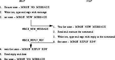
Detailed descriptions of FEP I/O library command and reply formats are provided in Section 39.0 . Detailed descriptions of the FEP Science command and reply formats are provided in Section 4.10 .
This section describes the structure of the FEP to BEP Science Data Ring-buffer. This buffer contains an array of TBD record structures, each of which consists of an array of 32 words.
TABLE 13. FEP to BEP Science Ring-Buffer Format
----------------------------------------------------------------------------------------------- Field Type Range Description----------------------------------------------------------------------------------------------- Write unsigned 0:records This field is an index into the ring buffer data area just Index in ring beyond the last written location. This index wraps to 0 buffer - 1 when it reaches the end of the buffer. This field must only be modified by the FEP. If this value is equal to the Read Index, then the ring-buffer is empty. If this value is one less than the Read Index (or at its greatest value if the Read Index is 0), then the ring buffer is full, and no more data can be written. Read unsigned 0:records This field is an index into the ring buffer data area just Index in ring beyond the last read location. This index wraps to 0 buffer - 1 when it reaches the end of the buffer. This field must only be modified by the BEP. Data record[TBD] : - This is an array of records, where each record is 32 Buffer where each words in length (32-bit words). This buffer must only record is be modified by the FEP. unsigned[32] -----------------------------------------------------------------------------------------------
 Next Chapter