Prior to shipment, MIT Lincoln Laboratories checks the output nodes of
each device for functionality and operates the devices at -40 C to verify
cosmetic quality. Once received at MIT CSR, the CCD is installed in a vacuum
chamber, the chamber is evacuated to a pressure of  torr,
and the device is cooled to -120 C.
The device is then exposed to an
torr,
and the device is cooled to -120 C.
The device is then exposed to an  Fe source to ensure that
it can detect X-rays and has no gross defects.
Fe source to ensure that
it can detect X-rays and has no gross defects.
Before the screening process begins, proper optimization of
the CCD's clock voltages must occur. The CCD biases which have the greatest effect
on device performance are drain bias applied to each of the four on-chip
MOSFET amplifiers. Indeed, we find that excellent device performance is
achieved with standard set biases for the charge transfer and reset clock voltages
for all devices. Thus, only the drain biases must be adjusted for each CCD. This
flexibility allows us to set charge transfer clock levels to maximal depletion
depth. Bias (source-free) and X-ray data (again
using an  Fe source) are taken over a wide range of clock voltages.
The Mn
Fe source) are taken over a wide range of clock voltages.
The Mn  and Mn
  lines provide a gain conversion and allow determination
of noise in electron units (see Section 3.4). During the subsequent screening and calibration
measurements, the CCD's clocks are operated at the voltages that produced
the lowest RMS noise.
lines provide a gain conversion and allow determination
of noise in electron units (see Section 3.4). During the subsequent screening and calibration
measurements, the CCD's clocks are operated at the voltages that produced
the lowest RMS noise.
Nominal operation of both ACIS-I and ACIS-S involves reading out each CCD through four output nodes in parallel in a timed exposure mode (time = 3.227 seconds for standard mode). During the course of the AXAF mission, however, other modes with different exposure times may be preferred for particular types of measurements. Continuous read-out modes (charge is continually clocked from the device) will be useful for observations where precision timing is important. Summation modes (blocks of pixels summed together and read out as a single pixel) exist to avoid pile up during observation of bright sources. Another mode variation allows the entire device to be readout through two output nodes (AC or BD). Reading out only a sub-array of the device reduces the integration time and permits observation of brighter sources. In total we examine eight different operational modes during the screening process. Table 1 lists each mode and briefly describes it.
Characterization of each readout mode requires several
measurements. Using a reflection grating monochromator, the CCD is illuminated with
monochromatic photons at the energy corresponding to the oxygen  line (525 eV)
and the aluminum
line (525 eV)
and the aluminum  line (1.49 keV). The device is also exposed to
Mn
line (1.49 keV). The device is also exposed to
Mn  and
and  lines produced by an
  Fe source. These
three measurements provide a determination of charge transfer inefficiency
(CTI), energy scale, and spectral resolution over a broad energy range
between .5 - 6 keV. Finally, dark current data are taken at a range of
integration times,
and a number of bias frames are taken. This procedure allows calculation of
the dark current present in the CCD.
Fe source. These
three measurements provide a determination of charge transfer inefficiency
(CTI), energy scale, and spectral resolution over a broad energy range
between .5 - 6 keV. Finally, dark current data are taken at a range of
integration times,
and a number of bias frames are taken. This procedure allows calculation of
the dark current present in the CCD.
A typical measurement begins by configuring the CCD to perform in a specific
mode by proper programming of the CCD clock sequencing electronics.
For the three spectral
resolution/CTI data sets, flux levels are checked and adjusted to
maximize incident flux consistent with acceptable pile-up.
We then collect enough data to
ensure that  photons are incident on each CCD quadrant. Bias
data is taken immediately preceding the collection of X-ray data. Finally,
the dark current data is taken.
Table 2 shows the typical
measurements made for each mode and the number of frames obtained.
photons are incident on each CCD quadrant. Bias
data is taken immediately preceding the collection of X-ray data. Finally,
the dark current data is taken.
Table 2 shows the typical
measurements made for each mode and the number of frames obtained.
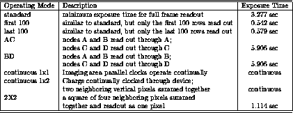
Table 1: Description of Readout Modes
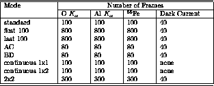
Table 2: Data Sets for Each Readout Mode
Analysis starts with the  Fe data set. The code subtracts bias levels
and corrects for drift in the overclocks before using
ASCA event detection and grading
algorithms to find events.
Event ``grades'' are assigned on the basis of the spatial charge distribution in
a 3x3 pixel neighborhood surrounding each event. Grades are used to select
events with well-collected charge.
Overclocks are thirty additional serial transfers that
occur after each row has been read out. Changes in overclock
levels indicate drift in the electronics.
The event list is then searched to locate hot
columns (defined as a column with a bias level 50 e
Fe data set. The code subtracts bias levels
and corrects for drift in the overclocks before using
ASCA event detection and grading
algorithms to find events.
Event ``grades'' are assigned on the basis of the spatial charge distribution in
a 3x3 pixel neighborhood surrounding each event. Grades are used to select
events with well-collected charge.
Overclocks are thirty additional serial transfers that
occur after each row has been read out. Changes in overclock
levels indicate drift in the electronics.
The event list is then searched to locate hot
columns (defined as a column with a bias level 50 e greater than
the median level), hot pixels (defined as a pixel with a
bias level 50 e
greater than
the median level), hot pixels (defined as a pixel with a
bias level 50 e greater than the median bias level), and bad columns
(defined as columns with low X-ray detection efficiency).
If any hot columns or hot pixels are found,
events from these columns are removed from the
greater than the median bias level), and bad columns
(defined as columns with low X-ray detection efficiency).
If any hot columns or hot pixels are found,
events from these columns are removed from the  Fe data and subsequent
data sets.
Fe data and subsequent
data sets.
With a properly corrected data set, noise, CTI, dark current, and spectral
resolution can be calculated. Noise is determined by computing the
pixel-by-pixel difference of two bias frames. A Gaussian is fit to the
histogram of this difference frame. The standard deviation of this
Gaussian is taken to be  time the RMS system noise.
Histograms are made of the graded events and used for CTI and spectral
resolution measurements. CTI is calculated by plotting
pulse height values versus row number (parallel CTI measurements) or
column number (serial CTI measurements), fitting a line of the form:
 to the data, and equating CTI to
  . Then a Gaussian is fit to the Mn k
 line to determine the
spectral resolution and energy scale of the CCD at 5.9 keV.
Each of these processing steps is repeated for the aluminum and oxygen
data sets in order to provide device-level performance information over
a broad energy band (0 to 5.9 keV). Section 5.2 contains sample data and plots.
line to determine the
spectral resolution and energy scale of the CCD at 5.9 keV.
Each of these processing steps is repeated for the aluminum and oxygen
data sets in order to provide device-level performance information over
a broad energy band (0 to 5.9 keV). Section 5.2 contains sample data and plots.
Dark current is calculated for modes with exposure times that can be varied.
An average bias frame is calculated from the dark current data
taken at the normal exposure time (3.277 seconds for standard mode). After the data has
been bias subtracted and overclock corrected,
an average pixel value is determined for each dark frame from a histogram of the pixels in
the image section. A linear relationship of the form:
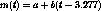 is fit to the data, where
 is the mean dark current in adu/pixel/sec and
  is the mode
bias value for a frame with integration time
is the mode
bias value for a frame with integration time  .
This value is converted from engineering units to
electron/pixel/sec using the gain values determined from the
.
This value is converted from engineering units to
electron/pixel/sec using the gain values determined from the  Fe
measurements.
Fe
measurements.
When the analysis has finished, the code processes the results and creates a summary sheet that details the CCD's performance and determines if it meets the acceptance criteria. This report presents all the relevant information in a readily digestible form and provides the ACIS team with the information needed to decide whether to fully calibrate a particular device. Figure 2 is the screening report for device c17-185-3. Besides displaying the measured quantities in tables, the summary sheet also lists the acceptance criteria and then decides if the device passed (P) or failed (F). The entire data acquisition and analysis process can be completed in about four hours.
Screening Report (FI) for c17-185-3 [T=-120.0 C]
(data_dir = /nfs/rico/d7/w185c3/23Jan96)
(output_dir = /ohno/da/Screen/c17-185-3/23Jan96/screen)
Fri Apr  5 14:56:38 EST 1996

Event Threshold = 100 ADU
Split Threshold:
     Node0: 13
     Node1: 13
     Node2: 12
     Node3: 13
Grade: cti(0-7); spec_resol(0,2-4); gain(0,2-4)

          <Readout Noise (noise[im]+d < 5 e-)>
Node(im)  Noise(electron)    Node(oc)  Noise(electron)     Test
-----------------------------------------------------------------
c0im    2.133 +/- 0.002     c0oc     2.084 +/- 0.007      P
c1im    2.735 +/- 0.003     c1oc     2.672 +/- 0.009      P
c2im    1.885 +/- 0.002     c2oc     1.812 +/- 0.006      P
c3im    1.904 +/- 0.002     c3oc     1.761 +/- 0.006      P

          <Parallel CTI [Fe55 at 5.9 keV] (< 5e-6)>
Node    CTI                                       Test
--------------------------------------------------------
c0      1.06836e-07 +/- 3.37265e-07               P
c1      6.86257e-08 +/- 3.38151e-07               P
c2     -2.11046e-07 +/- 3.28082e-07               P
c3     -1.13295e-07 +/- 3.49976e-07               P

          <Parallel CTI [O_k at 0.525 keV] (< 5e-5)>
Node    CTI                                       Test
--------------------------------------------------------
c0      8.01778e-06 +/- 1.87914e-06               P
c1      1.90632e-06 +/- 2.00573e-06               P
c2      7.50403e-06 +/- 1.80480e-06               P
c3      5.86082e-06 +/- 2.05938e-06               P

          <Serial CTI [Fe55 at 5.9 keV] (< 1e-5)>
Node    CTI                                       Test
--------------------------------------------------------
c0     -3.91665e-06 +/- 1.33823e-06               P
c1     -1.53416e-06 +/- 1.33965e-06               P
c2     -3.74164e-07 +/- 1.30727e-06               P
c3      1.37959e-06 +/- 1.35999e-06               P

          <Mean Dark Current (< 0.3 e/pix/s)>
Node    Dark Current (e/pix/s)     (95% uplimit)  Test
--------------------------------------------------------
c0    0.039285    +/- 0.000205    (0.220000   )   P
c1    0.034888    +/- 0.000254    (0.260000   )   P
c2    0.029906    +/- 0.000211    (0.220000   )   P
c3    0.070693    +/- 0.000202    (0.260000   )   P

          <Spectral Resolution [O_k at 0.525 keV] (FI:< 70eV)>
Node    FWHM(eV)                                  Test
----------------------------------------------------------
c0      44.3276     +/- 0.412155                  P
c1      48.4973     +/- 0.455946                  P
c2      43.8841     +/- 0.412187                  P
c3      42.9952     +/- 0.463458                  P

          <Spectral Resolution [Al_k at 1.487 keV] (FI:< 100eV)>
Node    FWHM(eV)                                  Test
----------------------------------------------------------
c0      67.4721     +/- 0.344109                  P
c1      69.5684     +/- 0.367777                  P
c2      67.093      +/- 0.363496                  P
c3      66.5883     +/- 0.385113                  P

          <Spectral Resolution [Fe55 at 5.898 keV] (< 165eV)>
Node    FWHM(eV)                                  Test
----------------------------------------------------------
c0      128.472     +/- 0.716822                  P
c1      129.882     +/- 0.726135                  P
c2      127.188     +/- 0.706473                  P
c3      127.231     +/- 0.729545                  P

          <Gain>
Node O_Gain(eV/ADU)           Al_Gain(eV/ADU)            Fe_Gain(eV/ADU)
-------------------------------------------------------------------------------
c0 4.07735 +/- 0.00187521    4.04416 +/- 0.000548207   4.05378 +/- 0.000287081
c1 4.14169 +/- 0.00204711    4.10557 +/- 0.000597824   4.11283 +/- 0.000293099
c2 4.53748 +/- 0.00206868    4.50461 +/- 0.000644549   4.508   +/- 0.00031659
c3 4.22243 +/- 0.00215265    4.1942  +/- 0.000632717   4.21641 +/- 0.000302656

<Hot Pixels>
     0 hotpixel
     0 hotcol
     0 hotpixel not in hotcol

<Bad Columns>
     0 badcol
Figure 2: Screening Report for device c17-185-3