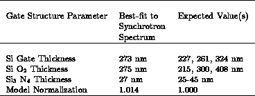
Table 3: Results of fits to synchrotron radiation spectrum
As is indicated in Figure 2, ACIS CCD quantum efficiency measurements are made in two phases. First, selected, flight-quality CCDs are calibrated absolutely with respect to synchrotron radiation (both undispersed and dispersed) of calculable intensity. We have used the facilities of the PTB Laboratory at BESSY for this purpose. The detectors calibrated at the synchrotron then serve as the reference standards with respect to which the flight detectors are calibrated.
A detailed discussion of the calibration of the reference detectors will be presented elsewhere; we simply summarize the method here, and provide illustrative results. The technique is similar to one used by Scholze and Ulm [15] to calibrate a Si(Li) detector. The basic premise is that the spectral energy distribution of the undispersed synchrotron radiation can, under appropriate conditions, be calculated with high accuracy from first principles. These conditions have been realized sufficiently well at the PTB Laboratory at BESSY [11] that uncertainties in the calculated flux can be reduced below 1%. If the spectral redistribution function of the CCD is sufficiently well-understood, then the response of the detector to the undispersed synchrotron radiation can be used to determine the parameters of the detector deadlayer. A secondary benefit of the synchrotron radiation is that the spatial variation of flux can be calculated, so the data may be used to constrain spatial variations in detector efficiency. In order to make use of the synchrotron radiation without saturating the CCD detector, it is necessary to operate the electron storage ring at extremely low current (literally a few to a few dozen electrons in the storage ring).
To illustrate the quality of the data that can be obtained with this technique, Figure 7 presents a measured pulse-height spectrum obtained at PTB, together with the response predicted by the best-fit model. The deviations of the model from the data are shown in the lower panel. The RMS deviation, as a fraction of the data, is 1.6% for this fit. The response model assumes that the gate structure is of piece-wise uniform thickness, while the real gate structure thickness varies from phase to phase. Some detector model parameters, such as the CCD depletion depth and channel stop dimensions, were held fixed at nominal values in this fit. As is shown in table 3, the best-fit mean deadlayer thicknesses agree well with scanning electron micrograph measurements of sibling devices. The best-fit overall normalization of the predicted spectrum agrees, within 1.4%, with the predicted flux.

Table 3: Results of fits to synchrotron radiation spectrum