Measurements made using the CCD aperture to restrict the X-ray
illumination to a spot on the CCD were performed by first aligning the
spot with two or three quadrants on the CCD, as shown in Figures 5 (Ti
K X-rays from HEXS aligned over quadrants A, B, and C) and Figure 8
(smaller spot of Mn K X-rays from an  Fe source, centered on
quadrants C and D). For the HEXS sources, the electron beam current
was adjusted to optimize the X-ray flux reaching the CCD. Next, the
SSD was moved into the beam for a pre-CCD measurement, integrating the
X-ray flux until typically 10
Fe source, centered on
quadrants C and D). For the HEXS sources, the electron beam current
was adjusted to optimize the X-ray flux reaching the CCD. Next, the
SSD was moved into the beam for a pre-CCD measurement, integrating the
X-ray flux until typically 10 counts were recorded in the main
photopeak. Then, the CCD aperture was returned to its original
position and the CCD data was acquired. Typically 600 frames of
duration 7.15 seconds were recorded from the CCD, along with 10 - 15
bias frames recorded prior to the X-ray exposure. Finally, the SSD
was moved back into position for a second post-CCD measurement,
similar to the first. Either the first or second SSD measurement was
broken into several segments in order to monitor the source stability
over time.
counts were recorded in the main
photopeak. Then, the CCD aperture was returned to its original
position and the CCD data was acquired. Typically 600 frames of
duration 7.15 seconds were recorded from the CCD, along with 10 - 15
bias frames recorded prior to the X-ray exposure. Finally, the SSD
was moved back into position for a second post-CCD measurement,
similar to the first. Either the first or second SSD measurement was
broken into several segments in order to monitor the source stability
over time.
In addition to the spot method, which uses the calibrated apertures to define the ratio of X-ray flux reaching the SSD and the CCD, a second full exposure method was used in which the SSD tube and CCD aperture piece were fully retracted out of the X-ray beam. This allows a full illumination of the CCD in order to evaluate the uniformity of response across the detector. Variations in detected intensity across the CCD are typically of order 1% [4]. A second measure of the CCDs average detection efficiency is obtained by normalizing its count rate by the ratio of the solid angles presented by the CCD surface and the SSD aperture as seen from the X-ray source. Uncertainties in the solid angles reduce the accuracy of this method (denoted as ``ALL'' in Table 1 below) as compared to that of the spot method, but it still provides a useful consistency check.
Typical spectral data from a low Z HEXS target material (Si) are shown
in Fig. 6 (measured by the SSD) and Fig. 7 (measured by one quadrant
of a CCD). For the Si source, the K (1.74 keV) and K
 (1.84 keV) lines are not fully resolved by either detector, although
the separation is clearer in the CCD response. In addition to the
main peak, a low energy tail is clearly seen in both graphs. These
spectra were fitted with two Gaussian components, a ramp-like tail
feature and a constant background. The two Gaussian peaks are
constrained to have widths and central positions in proportion to
those expected for the K
(1.84 keV) lines are not fully resolved by either detector, although
the separation is clearer in the CCD response. In addition to the
main peak, a low energy tail is clearly seen in both graphs. These
spectra were fitted with two Gaussian components, a ramp-like tail
feature and a constant background. The two Gaussian peaks are
constrained to have widths and central positions in proportion to
those expected for the K and K
and K lines, yielding a
reasonable fit to the blended peak. The low energy rise seen in the
CCD response, peaking at about 0.15 keV, is not due to electronic
noise. Rather, it is a real feature of the CCD response attributed to
incomplete charge collection for photons interacting near the
boundaries of the detecting silicon region.
lines, yielding a
reasonable fit to the blended peak. The low energy rise seen in the
CCD response, peaking at about 0.15 keV, is not due to electronic
noise. Rather, it is a real feature of the CCD response attributed to
incomplete charge collection for photons interacting near the
boundaries of the detecting silicon region.
Data at higher energies (Mn K lines from the  Fe source) are
shown in Fig. 9 (SSD) and Fig. 10 (CCD). Here the K
Fe source) are
shown in Fig. 9 (SSD) and Fig. 10 (CCD). Here the K (5.89
keV) and K
(5.89
keV) and K (6.49 keV) lines are well-resolved, and in addition
a Si escape peaks from both lines are visible at 4.15 and 4.65 keV. A
small Si K
(6.49 keV) lines are well-resolved, and in addition
a Si escape peaks from both lines are visible at 4.15 and 4.65 keV. A
small Si K peak is also visible in the CCD response at 1.74
keV, as is the Mn L feature at 0.64 keV and the low energy rise at
about 0.15 keV.
peak is also visible in the CCD response at 1.74
keV, as is the Mn L feature at 0.64 keV and the low energy rise at
about 0.15 keV.
These response curves demonstrate the superior resolution of the CCD as compared to the Si(Li) SSD, both at 1.74 keV (77 eV FWHM compared to 100 eV) and at 5.89 keV (132 eV compared to 141 eV). For single-pixel events only, the two CCD values fall to 74 eV and 125 eV. The differences are even larger when the low-noise ACIS design electronics are used to read the CCD.[3][13]
A full analysis of the detection efficiency of the ACIS reference CCDs
has not yet been completed. As discussed above, X-rays detected by
the CCD are separated into grades according to how the charge is
distributed among neighboring pixels; therefore detection efficiencies
must be determined from counting rates in each grade and grade
branching ratios. The effects of pile-up on the CCD count rate must be
accounted for, and detailed response functions appropriate for both
the SSD and the CCDs must be fitted to the measured spectra. Pile-up
can both give multi-photon events (combining the energy of two or more
photons) and cause a loss of counts due to ungraded charge
distributions covering five or more pixels. While our X-ray flux is
set to minimize pile-up, some level of this phenomenon is unavoidable
for reasonable counting rates. Typically, pile-up affects 5% or less
of the events and its effect is calibrated to a level of 10%,
contributing an uncertainty of  or less.
Preliminary analysis of the data has been performed using a simple comparison of counts in the main photopeaks in the measured spectra of the SSD and the CCDs. These results are presented in Table 1, which shows the ratio of counting rate in the CCD (for 1- and 2- pixel events only) to that of the Si(Li) SSD. The SSD has been corrected for the estimated transmission of the Be window and the Au/Pd contact layer, and the ratio of the two aperture areas has also been included in measurements labeled ``ABC'' etc (quadrants illuminated by the spot method). A more detailed analysis including counts in the low energy tail and any escape peaks is pending.

Figure 5: Uniformity of Ti X-rays illuminating CCD quadrants A, B and C.
Contour lines indicate levels of 1%, 5%, 10%, 50% and 90% maximum
intensity.

Figure 6: Response of the Si(Li) solid state detector to
Si K X-rays (1.74 and 1.84 keV).
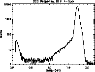
Figure 7: Response of an ACIS CCD to Si K X-rays (1.74 and 1.84 keV).

Figure 8: Uniformity of  Fe X-rays illuminating
CCD quadrants C and D.
Contour lines indicate levels of 1%, 5%, 10%, 50% and 90% maximum
intensity.
Fe X-rays illuminating
CCD quadrants C and D.
Contour lines indicate levels of 1%, 5%, 10%, 50% and 90% maximum
intensity.
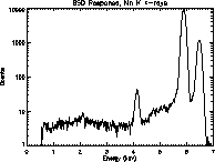
Figure 9: Response of the Si(Li) solid state
detector to Mn K X-rays (5.89 and 6.49 keV).
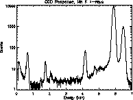
Figure 10: Response of an ACIS CCD to Mn K X-rays (5.89 and 6.49 keV).
The precision of the data in Table 1 is not intended to imply absolute accuracy but to convey the uniformity of results across different quadrants and different CCDs. Data from different quadrants on the same CCD generally agree to the 1% level or better. Measurements labeled ``All'' represent estimates from the full illumination method, and are typically within 3% of the spot measurements. These ``All'' measurements have higher uncertainty due both to solid angle estimates and to the untested assumption of uniform illumination across the CCD. As mentioned above, photon statistics contribute an uncertainty of order 0.35% or less to each measurement.
At higher energies, the drop in detection efficiency for the CCDs is due in part to X-rays that pass through the depletion depth without interacting, but also to the higher branching ratio of 3- and 4-pixel events. These events are not included in the efficiency values presented.

Table 1: Ratio of CCD Detection Efficiency
(one- and two- pixel events only) to SSD Detection Efficiency. Only
counts in the main photopeaks of each detector were used for this
preliminary analysis. Estimated uncertainty due to photon statistics
is  .
.
The lower energy measurements (Si and P) are heavily weighted to single and double pixel events, and will be used for comparison to calibration measurements made at the PTB/BESSY facility (whose analysis is also in process). The uncertainty in the SSD calibration at these lower energies is larger due to the higher attenuation of the window and contact layer of the SSD, as well as the higher fraction of events that show up in the low energy tail of the SSD response. Modeling and fitting this tail component is inherently more difficult than fitting the main Gaussian photopeak. Consequently, the BESSY calibration will be our primary standard for energies below 3 - 4 keV. Indeed, the BESSY data indicates that the detection efficiency values at 1.74 and 2.01 keV are lower than the ratios given in Table 1.
Two approaches for refining our knowledge of the SSD response are under consideration. In one case, we could calibrate the SSD itself at the PTB/BESSY facility, or by comparison with another AXAF transfer standard that has already been so calibrated. A newer beamline at BESSY has recently become available with known spectral radiance at energies exceeding 10 keV, which would allow all of the ACIS CCD calibration measurements to be tied to this standard. A second approach is to utilize the SSD and BESSY results at 1.74 and 2.01 keV to fit the uncertain SSD parameters (contact layer, Be window thickness, possible dead layer thickness). These parameters would then constrain the SSD detection efficiency at the higher energies, and by comparison the CCD detection efficiency values as well. In either case we also plan to further refine the response function models for both the SSD and the CCDs, which will allow us cast the detection efficiency parameters into the framework of NASA's XSPEC code.