Next: 2.3.7.3 DPA Hardware Recovery Up: 2.3.7 DPA Hardware Previous: 2.3.7.1 Introduction
Next: 2.3.7.3 DPA Hardware Recovery
Up: 2.3.7 DPA Hardware
Previous: 2.3.7.1 Introduction
All processors in the DPA have identical cores: the MIPS3000 RISC CPU as implemented by LSI. It is commonly called the `Mongoose'. This is a radiation resistant (Rad-hard) version of the LSI Logic LR33000 (Self-Embedding Processor) which is adapted to the special requirements of space-systems electronics.
The `Mongoose' forms the heart of the DPA processors. The chip itself includes an interrupt controller, a DMA controller, timer/counters, a serial port/debug interface, and cache control. The rest of the electronics contains processor support logic, memory, and dedicated interface circuits. The Mongoose requires little support logic. It has an internal interrupt controller with eight independent interrupt lines. An internal UART is provided. An internal DMA controller allows for autonomous memory to memory data transfer.
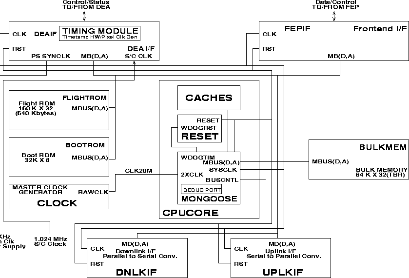
The BEP block diagram is shown in Fig. 2.24. There are three 32-bit busses on the BEP boards, all connected to the Mongoose. The I-bus is the Instruction Cache Bus, consisting of 32 bits of data and 20 bits of addresses, accessible via words only. The D-bus is the Data Cache Bus, consisting of 32 bits of data and 20 bits of address, again accessible only via words. The M-bus is the Memory Bus, consisting of 32 bits of data and 29 bits of address, accessible by words or bytes.
Cached execution allows the Mongoose to take advantage of the `Harvard Architecture' to simultaneously fetch from the data bus and the instruction bus. All Mongoose instructions are 32-bits, and will normally require one clock cycle.
The M-bus is a general purpose peripheral bus with configurable wait states. Use of the M-bus can slow processor operation due to pipeline stalls.
The BEP has a 512 kByte instruction cache in RAM. This RAM has 35 ns access time to support the 10 MHz Mongoose. The RAM is extremely Rad-hard and SEU (Single Event Upset) immune RAM. The BEP has a 256 kByte data cache. Like the instruction cache, the memory is 35 ns and Rad-hard SRAM.
Bulk memory on the BEP is used for buffering downlink packets before transmission to the RCTU. The planned storage is 256 kByte. This amount of storage will buffer almost 10 exposures of event lists at the maximum data rate in faint mode.
The flight software ROM contains a non-volatile copy of both the FEP and BEP flight software. It is currently sized at 1 MByte, with 512 kByte for the BEPs and 128 kByte for the FEPs. The ROMs will be the same used for the Boot ROM.
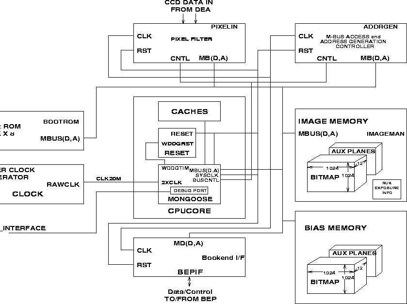
The FEP block diagram is shown in Fig. 2.25.
The FEP is a the processor which services (at any
one time) a single CCD. Digitized pixel data arrives at
the rate of one 12-bit word per 2.5 ![]() sec. The FEP
must process this data real-time, and reduce it to a
candidate event list, which is sent to the BEP. The FEP
contains dedicated hardware which works in parallel to
the software, filtering pixel data in order to relieve the
load on the processor, and thus meeting the speed requirements
on the system.
sec. The FEP
must process this data real-time, and reduce it to a
candidate event list, which is sent to the BEP. The FEP
contains dedicated hardware which works in parallel to
the software, filtering pixel data in order to relieve the
load on the processor, and thus meeting the speed requirements
on the system.
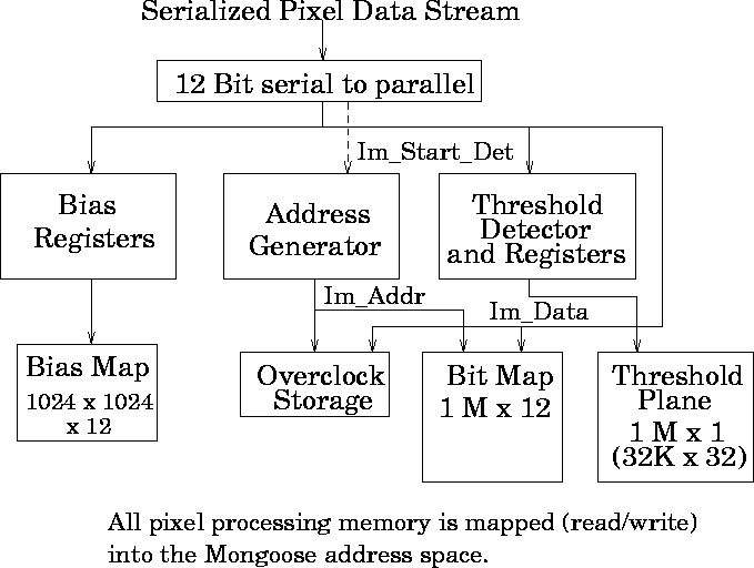
This dedicated hardware operates on a pixel-by-pixel basis, selecting potential events based on threshold crossings. It also characterizes the dark level of the CCD by generating bias maps of the CCD pixel outputs.
The core processor and busses are identical on the FEP and BEP. Only differences will be mentioned in the following FEP description.
The processor core and bus of the FEP differs from the BEP only by the smaller instruction cache. 128 kBytes of SRAM will be used by the FEP. The pixel processing hardware detects events in the raw pixel stream of 1024x1024x12-bits in each 3.3 sec exposure. The frontend hardware performs the threshold crossing detection and relays this information to the Mongoose.
Figure 2.26 shows the logical flow of interrelations in the pixel processing hardware.
John Nousek