Next: 2.3.7 DPA Hardware Up: 2.3.6 DEA Hardware Previous: 2.3.6.2 Interfaces
Next: 2.3.7 DPA Hardware
Up: 2.3.6 DEA Hardware
Previous: 2.3.6.2 Interfaces
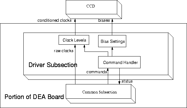
The Driver Section is responsible for controlling the CCD clock levels and biases as specified by the DPA. Figure 2.20 illustrates the major functions of the Driver Section. The BEP on the DPA sends commands to the Driver Section via the Common Section. These commands control the bias levels and clock levels sent to the CCD. The Driver drives the conditioned CCD clocks using the raw clock timing signals generated by the Common Section's Sequencer.
In more detail, the Driver decodes, executes, and communicates commands from the DPA via a resident Field Programmable Gate Array (FPGA) chip. After the command is decoded, control signals are generated and distributed throughout the driver section to execute various functions as instructed by the command for proper CCD Driver operation. This chip controls the Digital to Analog Converter (DAC) banks, which determine the CCD clock and bias amplitude voltages. These values are conditioned (i.e., amplified, filtered, and regulated) before being passed on to the CCD. Timing information is impressed upon the clock amplitudes via a switching network, which is generated by the Common Section.
The Driver Section also has the ability to monitor signals which can determine the overall functional health of the Section (housekeeping).
Video Section
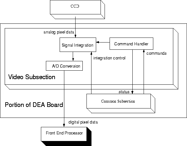
The Video Section samples and digitizes the analog CCD pixel data and sends the converted data back to the DPA's Front End Processors for further processing. Figure 2.21 illustrates the major components of the Video Section. This Section integrates the signal from the CCD via the integration control signals provided by the Common Section's sequencer. The Video Section converts the integrated analog signal to a digital pixel pulse height and sends the data to one of the DPA's FEPs to be processed.
The Video Section shares a FPGA chip with the Driver Section to control all command decoding, execution and communication with the DPA. These instructions enable acquisition and digitization of the CCD video outputs.
The Video Section contains four independent video chains which process the four sections of a CCD simultaneously. All four video chains require individual offset voltage control. These offset voltages are determined by a set of DAC banks, which are set by the FPGA chip as instructed by DPA commands.
Also like the Driver Section, the Video Section provides housekeeping signals. The power conditioning network on the analog board has the ability to shut down its rail potentials when excessive current is being drawn. This provides a safety feature to prevent overcurrent and failure as a result of a ``latch-up''. Depending on the readout mode specified upon initialization, the power on the video chains A and C or B and D can be independently shut down to conserve power.
The Video Section acquires and digitizes four pixels in parallel, each pixel signal coming from one of four output nodes of a CCD. The acquisition process is synchronized with the CCD clocks via the Analog Sequence Bus generated by the Common Section. The X-ray-induced signals are extracted from high noise and bias voltage levels and passed on to the pre-amp before digitization. The pre-amp can introduce a programmable offset voltage to the data as well as reducing the gain from 1 ADU/e- to 0.25 ADU/e-. The data are then digitized, with digital conversion synchronized with the CCD clocks and controlled by timing signals sent from the Common Section. The four video channels are multiplexed into one data stream, which is then synchronized to the BEP clock.
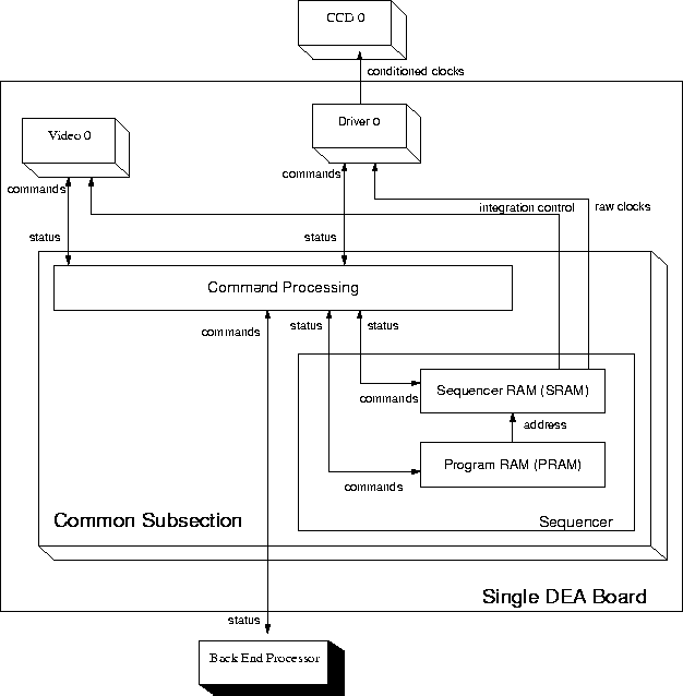
As illustrated in Figure 2.22, each Common Section contains a command processor, which receives commands from the BEP, executes commands addressed to it, and dispatches commands to the addressed Video or Driver Section. Status from the executed command is then returned to the BEP. Each Common Section also contains a CCD Sequencer. The Sequencer contains an array of 16-bit SRAM words and an array of PRAM words. The SRAM and PRAM control the sequencing of the corresponding CCDs.
Each bit in an SRAM word corresponds to a single CCD clock or control signal. When a word is `executed,' each bit of the word drives its corresponding signal to either a `high' or `low' state. When the Sequencer runs a block of SRAM, it fetches and `executes' each word in sequence. The time between each word is constant and is determined by the Sequencer clock. The BEP is responsible for sending commands to the Common Section to load PRAM and SRAM.
Common Section
The Common Section dictates all intersectional synchronization and sequencing of a DEA subsystem. Its main function is to generate synchronized timing signals and to distribute them via the Analog Sequencer Bus to the Driver and Video Sections. The sequencer signals going to the Driver Sections effectively transport pixel charge from the CCDs to the video processing chains in an ordered manner. The sequencer signals going to the Video Sections synchronize the acquisition and digitization of the pixel charge.
All commands to any particular subsystem go through the Common Section first and then fan out to all its associated Driver and Video Sections. The global housekeeping ADC is on an eleventh board in the DEA, whereby all the multiplexed intersectional housekeeping channels arrive and are converted as status data upon command.
A board level conditioning network on the Common Section has the ability to shut down when excessive current is being drawn. This provides a safety feature in preventing a catastrophic ``latch-up''.
John Nousek