Next: 2.3.6.2 Interfaces Up: 2.3.6 DEA Hardware Previous: 2.3.6 DEA Hardware
Next: 2.3.6.2 Interfaces
Up: 2.3.6 DEA Hardware
Previous: 2.3.6 DEA Hardware
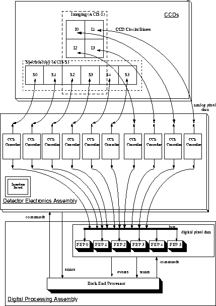
The DEA (Detector Electronics Assembly) is the direct electronic interface to the CCDs, providing all the circuitry needed for their operation and to receive their analog output. It provides the clocking information for the CCDs and digitizes the analog pixel data, sending this digitized stream to the Digital Processing Assembly (DPA) for event recognition and processing.
The DEA consists of ten independent, identical subsystems, each controlling a single CCD. A complete subsystem consists of three sections: a `driver' section, a `video' section, and a `common' section. It requires the interaction of all three sections to service one CCD. The driver section provides signal levels, conditions the clock signals delivered to the CCD, and controls the CCD bias. The video section is responsible for amplifying, sampling, and converting analog video data from the CCD into a digital format. This section provides the Front End Processors (FEP) of the DPA with raw digital CCD pixel data for processing. The common section is responsible for receiving and dispatching commands from the Back End Processors (BEP) of the DPA, and for managing the CCD clock sequencing.
Figure 2.19 illustrates the main components of the DEA and how each component maps to its respective CCDs and to the components of the DPA. There are 40 analog signal chains, one for each CCD output node (with four output nodes on each chip). At any one time, at most 24 analog signal chains are in use. These in turn are multiplexed to six frontend processing chains (one for each FEP - see Section 2.3.7).
John Nousek