Next: 2.2.2 Mechanical Up: 2.2.1 Optical Previous: 2.2.1 Optical
Next: 2.2.2 Mechanical
Up: 2.2.1 Optical
Previous: 2.2.1 Optical
The ACIS active sensors consist of two independent arrays
of Lincoln Lab framestore CCD chips, one optimized for imaging
performance over the entire array (ACIS-I) and the other optimized for
spectral resolving power of the combined ACIS/HETG/HRMA system (ACIS-S).
The center unit of the second array also serves as the optimum detector
for reduced field imagery and will be the launch-lock position.
A mixture of frontside illuminated and backside illuminated
CCD chips is used in the ACIS-S array, each chip having an X-ray sensitive
active area consisting of a planar, roughly 2.4 cm square
(![]() cm2).
cm2).
The rationale for requiring the two arrays is as follows. The ACIS-I array provides the best imaging performance over the widest possible field allowed by the HRMA optical properties. The difference between the ACIS-I array and a flat detector or the ACIS-S spectroscopic array corresponds to a factor of up to two in the angular resolution of the instrument over the entire field of view, which leads to a factor of four in the limiting sensitivity for detecting sources under some conditions. Additionally, the three-dimensional spatial positioning of the chips in the ACIS-I array leads to nearly complete coverage of the entire HRMA focal surface for which the blur circle is 5 arc-sec or less. The ACIS-S array has less than half the coverage on the sky (field of view) at this performance.
On the other hand, ACIS-S is essential for meeting the needs of the grating readout. The grating focal surface is nearly flat, so trying to use ACIS-I as a readout for the gratings would lose the same factor of two in angular resolution, and therefore spectral resolution, which the ACIS-S array loses when used for imaging. (Note that grating spectral resolving power is directly related to angular resolution.) Additionally, a large array in one dimension is needed for wavelength coverage, so ACIS-I would only cover 1/3 of the spectral band that ACIS-S will cover. However, the flat nature of the ACIS-S array is not a drawback for reduced field imaging applications where field of view is less important. Thus in cases where the presence of the gaps between chips will be undesirable, but the size of the field of view is small, ACIS-S may be preferable for imaging applications. Another application of ACIS-S would be for observations which require the preservation of the symmetry of the point spread function for targets near the telescope axis. Finally, only ACIS-S contains BI CCD chips, so in those cases where detection or imaging of soft spectrum sources is required ACIS-S must be used.
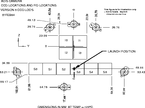
To achieve these goals, ACIS-I consists of four CCD chips
tipped in two dimensions so as to form a shallow 2x2 bowl. The
center of the active area of each chip lies approximately
on the tangent to a 250 mm radius sphere.
(See Fig. 2.11 on page ![[*]](/images/LatexHtml/cross_ref_motif.gif) for an isometric projection of this array as an aid in visualization.)
for an isometric projection of this array as an aid in visualization.)
The ACIS-I CCD chips are butted as closely as possible, with gaps not exceeding 0.54 mm spacing. The framestore portions of the chips project outward from the center of the array, roughly orthogonal to both the HRMA axis and the direction of SIM translation.
The ACIS-S array consists of six chips butted so that
their active areas form a single one-dimensional array of chips.
The framestore areas project along the SIM translation direction,
perpendicular to the HRMA axis.
(See Fig. 2.12, page .)
When focused by the SIM translation
and axial focusing motion, the mechanical alignment is such that the
HRMA axis intersects the array 6.25 mm in from the seam between
the third and fourth chips in the row. These seams are as small
as possible, but no larger than 0.431 mm. The ACIS-S array chips are very
slightly, and progressively, tipped to approximate the Rowland Circle
of the gratings. The center of each chip is positioned at the tangent
point to a cylinder of radius of roughly 4325 mm,
with the on-axis focal spot falling directly on the surface of the chip
to provide optimum focus over the entire dispersed spectrum.
 |
The spacing between the ACIS-I and S arrays is set at 8 mm, in order to allow space for filter support structures, without blocking or vignetting the field of view of either array.
The internal alignment of the ACIS experiment is determined on-orbit by knowledge to 0.1 mil of the fiducial light reference system over at least 85% of the orbit. The anticipated time interval when internal ACIS alignment will degrade is during the six hours nearest perigee passage.
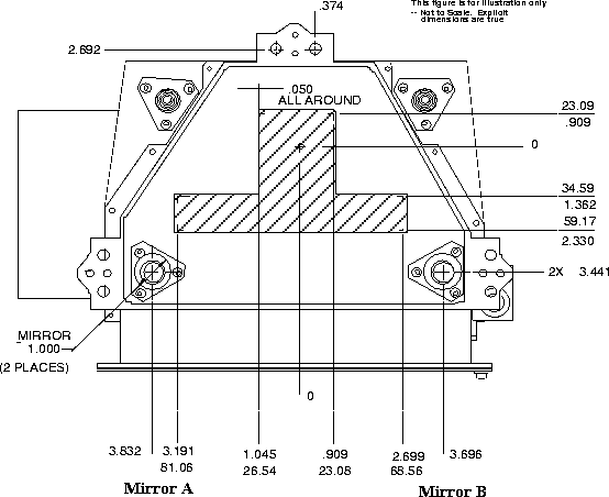
The external alignment knowledge that is relevant to ACIS performance is the relation between the active areas of the CCD chips in the I and S arrays and the HRMA optical coordinate system. This alignment is maintained by co-aligning both the ACIS-I and S arrays with the system of six fiducial lights. The ACIS-I and S arrays are mechanically part of a single structure, the Focal Plane (FP), which must be correlated to the coordinate system defined by the centroid of the fiducial light system. The knowledge of the position of ACIS with respect to AXAF is determined via two reference mirrors mounted on the front of the detector housing.
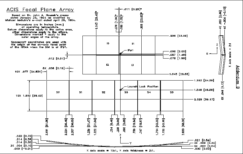
Mechanical fabrication will place the ACIS focal
plane at the designed location. Offsets of the focal plane
from the position of alignment mark inscribed on the
alignment mirrors mounted to the detector housing are then measured. Nominal
locations of the mirrors and fiducial marks are shown in
Figures 2.3 and 2.4.
The positional tolerance on the alignment mirrors
is ![]() inch.
inch.
The full alignment involves four steps. Each CCD chip
active area is mounted into the FP structure such that the four
corners are positioned as closely as possible to
the focal plane coordinates specified
in Figure 2.5. These positions are checked using
microscopy to within 7.6 ![]() m in Y and Z, and 25
m in Y and Z, and 25 ![]() m in
X (HRMA focus). The positions of the CCDs are used to determine
the actual focal surface which is then related to an orientation mirror
which is attached to the FP structure. This mirror
has its normal determined within 2 arcsec.
m in
X (HRMA focus). The positions of the CCDs are used to determine
the actual focal surface which is then related to an orientation mirror
which is attached to the FP structure. This mirror
has its normal determined within 2 arcsec.
Four thermoplastic standoffs mechanically hold the
FP structure to the detector housing. The alignment between
the fiducial marks on the mirrors on the exterior of the detector
housing and the FP coordinate system will be better than 100 ![]() m
in X and 25
m
in X and 25 ![]() m in Y and Z. The normals of the exterior
mirrors shall be correlated to within a few arc-sec of the FP coordinate
system defined by the focal plane mirror.
m in Y and Z. The normals of the exterior
mirrors shall be correlated to within a few arc-sec of the FP coordinate
system defined by the focal plane mirror.
Positioning the ACIS is achieved by mechanical attachment of the detector housing to the SIM. Alignment is achieved by use of shims placed between the mounting feet of the collimator and the SIM.
Focussing of the ACIS instrument can be achieved via two complementary techniques. Shutter focus can only be done in the XRCF calibration facility. All except one quadrant of the mirrors were covered by closed shutters. The resulting out-of-focus image appears like a pie-shaped quadrant, which has a centroid displaced toward the open shutter quadrant if the detector is closer to the mirrors than the focus, and displaced away from the open quadrant if the detector is farther than the focus. The amplitude of the displacement is proportional to the distance out of focus.
The shutter focus procedure consists of collecting images from all four open quadrants sequentially, then changing the axial displacement of the detector to the opposite side of the focus point and repeating the measurement. The signs of the displacements should all flip, and by interpolating the common measurements the point of flipping can be independently determined from all four quadrants. Typically the detector is then moved to the interpolated focus point and one more shutter sequence is done, checking that no significant displacement of the image occurs, confirming the focal point.
In orbit no shutters are present. The focus determination is done by minimizing the variance (second moment) of the image as a function of axial displacement. Several axial points are measured and a parabolic fit made to determine the minimum. Note that this approach is slower because more points must be measured and that more photons are needed to accurately measure the variance as opposed to the centroid of a distribution.
Stray light (i.e. light at any wavelength which strikes the ACIS CCD chips without being brought to a focus by the HRMA) represents a source of potential signal degradation to ACIS. Although individual photons of UV or longer wavelength cannot be individually recognized by ACIS their presence increases the effective readnoise, and hence degrades the energy resolution of the instrument.
The optical blocking filter substantially reduces the UV/optical
flux, but in order to eliminate the deleterious effects of
stray light it is necessary to limit the stray light striking
the CCDs to less than 1 photon per pixel per readout.
This level is met by an AXAF Observatory stray light requirement
to limit the maximum ACIS irradiance by stray light to less than
![]() photons-cm2-s-1 over the band
3000 Å to 11000 Å. In addition over the UV range (100 Å to 3000 Å) solar flux must be attenuated by at least 1010
and bright Earth flux must be attenuated by at least 107.
photons-cm2-s-1 over the band
3000 Å to 11000 Å. In addition over the UV range (100 Å to 3000 Å) solar flux must be attenuated by at least 1010
and bright Earth flux must be attenuated by at least 107.
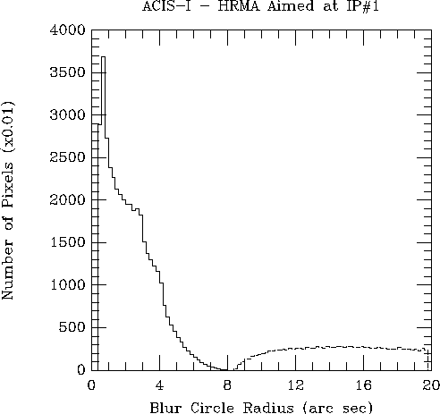 |
The image quality depends upon the mirror type and figure, the ACIS geometry, and detector location and orientation. The four imaging CCDs are not co-planar, but crudely tile the focal surface. A figure of merit is shown in Figure 2.6, which displays the number of pixels for which 68% of the encircled energy is within the radius specified on the horizontal axis -- over 50% of the array is better than 2 arc-sec, and 90% of the array has better than 4 arc-sec imaging. (As the mirror shells have different effective area with energy, the blur performance is energy dependent. Fig. 2.6 is calculated in the low energy limit.) This figure includes the intrinsic blur of the HRMA. Other sources of blurring - misalignments (ACIS-HRMA axes; ACIS tilt; HRMA focus) and time-resolution (if the aspect changes over the exposure interval, for example) -- are estimated to amount to about 0.3 arc-sec (which add in quadrature, if random, to the data in Figure 2.6).
The total field of view of each array is set by the plate scale
of the optical system, which makes each pixel cover 0.49 arc-sec
square regions on the sky. After allowing for the
narrow gaps between the CCD chips the imaging array covers
a total field of view of roughly 16.9 arc min square.
Vignetting reduces the effective area of the telescope
as the off-axis angle increases, and the imaging performance
also degrades.
For a more detailed discussion of the imaging properties of the
separate arrays see Sec. 2.3.2.2,
page .
As ACIS can operate up to six CCD chips in parallel, it is possible to include two ACIS-S chip outputs when ACIS-I is located at the HRMA focus. Although the image performance of these two chips will be worse than the ACIS-I chips because of the large off-axis angle, these chips add 50% to the total sky coverage of ACIS in this mode. The blur performance of these chips is shown by the broken line histogram in Fig. 2.6.
John Nousek