Ionizing x-rays are provided by a commercial x-ray tube with a maximum
voltage and power capability of 30 kV and 9 W. The tube is model
TFS-5109 manufactured by TruFocus Corp.[3] The tube has a
takeoff angle of  , a molybdenum target, and a 0.005'' Be
window. The tube is powered by a Spellman power supply [6]
SL30P10/FPS/X2130, with a 30 kV capability. The Spellman power supply
is especially modified for use with the TruFocus tube. The x-ray tube
is housed in a vented brass box for radiation protection, which is
connected to a vacuum system containing a fluorescent target chamber
and CCD detector, as shown in Fig. 1. X-rays are emitted from the
TruFocus tube through a 1/8'' diameter aperture, and exit the brass
box in an aluminum-lined 1/4'' diameter aperture. The target chamber
vacuum interface lies 12 cm beyond. X-rays enter that chamber through
a 1/2'' dia. Be window of thickness 0.005''. A fluorescing target
lies 14 cm beyond the Be window so that the distance between the
tube's molybdenum target and the fluorescing target is 34 cm. Of this
distance, 17.5 cm is air at 1 atm. A 8.8 mm diameter aperture lies
between the x-ray tube and the fluorescing target to limit the x-ray
beam to only fall on the target. The target itself lies on one face
of a vertical, square rotatable bar of solid aluminum (1 inch on a
side). The bar can also by withdrawn 2 inches in the vertical
direction to expose addition targets. Thus, twelve different target
materials may quickly be presented to the x-ray beam without breaking
vacuum. Normal operation has the target face oriented with a
45
, a molybdenum target, and a 0.005'' Be
window. The tube is powered by a Spellman power supply [6]
SL30P10/FPS/X2130, with a 30 kV capability. The Spellman power supply
is especially modified for use with the TruFocus tube. The x-ray tube
is housed in a vented brass box for radiation protection, which is
connected to a vacuum system containing a fluorescent target chamber
and CCD detector, as shown in Fig. 1. X-rays are emitted from the
TruFocus tube through a 1/8'' diameter aperture, and exit the brass
box in an aluminum-lined 1/4'' diameter aperture. The target chamber
vacuum interface lies 12 cm beyond. X-rays enter that chamber through
a 1/2'' dia. Be window of thickness 0.005''. A fluorescing target
lies 14 cm beyond the Be window so that the distance between the
tube's molybdenum target and the fluorescing target is 34 cm. Of this
distance, 17.5 cm is air at 1 atm. A 8.8 mm diameter aperture lies
between the x-ray tube and the fluorescing target to limit the x-ray
beam to only fall on the target. The target itself lies on one face
of a vertical, square rotatable bar of solid aluminum (1 inch on a
side). The bar can also by withdrawn 2 inches in the vertical
direction to expose addition targets. Thus, twelve different target
materials may quickly be presented to the x-ray beam without breaking
vacuum. Normal operation has the target face oriented with a
45 angle of incidence and emission with respect to the x-ray
tube and CCD, respectively. The CCD lies about 60 cm away from the
fluorescing target and is baffled with a 1.6 cm diameter aperture
so that only the fluorescing target has a line-of-sight to the
CCD (conversely, all portions of the CCD view all portions of the
fluorescing target). All critical surfaces and apertures are lined
with aluminum to minimize excitation of contaminating high energy
x-rays. The 12 different targets used for our CCD calibration are
aluminum, silicon, phosphorus, potassium chloride, titanium, vanadium,
iron cobalt, nickel, copper, zinc, and germanium.
angle of incidence and emission with respect to the x-ray
tube and CCD, respectively. The CCD lies about 60 cm away from the
fluorescing target and is baffled with a 1.6 cm diameter aperture
so that only the fluorescing target has a line-of-sight to the
CCD (conversely, all portions of the CCD view all portions of the
fluorescing target). All critical surfaces and apertures are lined
with aluminum to minimize excitation of contaminating high energy
x-rays. The 12 different targets used for our CCD calibration are
aluminum, silicon, phosphorus, potassium chloride, titanium, vanadium,
iron cobalt, nickel, copper, zinc, and germanium.
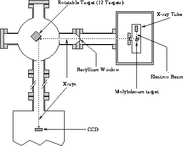
Figure 1: Basic schematic of high energy x-ray source (HEXS).
It is important to have a theoretical description of the physics of x-ray emission so as to understand the x-ray emission rate. Electron bombardment of a material produces both continuous (bremsstrahlung) and line radiation. An analysis of the continuous spectrum starts with Kramer's Rule[7] which states that the locally generated x-ray photon number spectrum by a single electron on a thick target is

where  is the incident electron voltage
and Z is the target atomic number. In reality, the numerical factor is
a slowly varying function of E and Z. For molybdenum[8]
(z=42),
is the incident electron voltage
and Z is the target atomic number. In reality, the numerical factor is
a slowly varying function of E and Z. For molybdenum[8]
(z=42),  . More accurate modern analyses
including corrections for internal absorption and electron backscatter
have been developed. Using the approach by Pella, et al,[9] a
theoretical to experimental comparison of the x-ray spectra emerging
from the molybdenum x-ray tube and incident on a target material is
shown in Fig. 2. The model gives the x-ray spectra in terms of
incident photons per CCD per keV per 10
. More accurate modern analyses
including corrections for internal absorption and electron backscatter
have been developed. Using the approach by Pella, et al,[9] a
theoretical to experimental comparison of the x-ray spectra emerging
from the molybdenum x-ray tube and incident on a target material is
shown in Fig. 2. The model gives the x-ray spectra in terms of
incident photons per CCD per keV per 10  A, and includes all
attenuations due to the beryllium windows and air. The solid line is
the experimental spectrum taken with a CCD, and the lightly dotted
line is the model spectrum, which also includes a simple CCD model.
The x-ray tube voltage and current for this particular example are 15
kV and 10
A, and includes all
attenuations due to the beryllium windows and air. The solid line is
the experimental spectrum taken with a CCD, and the lightly dotted
line is the model spectrum, which also includes a simple CCD model.
The x-ray tube voltage and current for this particular example are 15
kV and 10  A, respectively. The tall peaks around 2.2 keV are
molybdenum L lines, while the peak at 1.7 keV is the silicon escape
peak.
A, respectively. The tall peaks around 2.2 keV are
molybdenum L lines, while the peak at 1.7 keV is the silicon escape
peak.
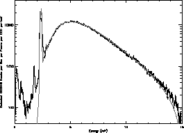
Figure 2: X-ray spectrum incident on target assembly.
Once the incident spectrum on a target material is known, it is
possible to calculate the outgoing flux of fluorescent K radiation. See Van Grieken[10] for a summary. The physics is
straightforward once given the incident x-ray spectrum: for an
incident monochromatic x-ray beam of intensity
radiation. See Van Grieken[10] for a summary. The physics is
straightforward once given the incident x-ray spectrum: for an
incident monochromatic x-ray beam of intensity  (photons/sec/steradian/eV) on a thick
homogeneous target, the outgoing K
(photons/sec/steradian/eV) on a thick
homogeneous target, the outgoing K intensity is

where
 is the photoelectric absorption cross section,
  is the fluorescent yield,
  is the probability for K
 emission (as opposed to K
 ), j is the ``jump factor'',
  is the mass absorption coefficient,
  and
and  are the
respective incident and takeoff angles for the photons with respect to
the surface,
are the
respective incident and takeoff angles for the photons with respect to
the surface,  is the incident x-ray energy, and
  is the
emitted K
is the
emitted K energy. This formula does not include geometry
factors and detector efficiency. It remains to integrate this
expression over the appropriate energy range of the incident x-ray
spectrum to obtain the entire K
energy. This formula does not include geometry
factors and detector efficiency. It remains to integrate this
expression over the appropriate energy range of the incident x-ray
spectrum to obtain the entire K flux.
flux.
HEXS has been tested with twenty different target elements or
compounds at all atomic numbers ranging from Z=9 (lithium fluorine) to
Z=32 (germanium), except neon, argon, manganese, and gallium. The
detected x-ray flux on a CCD from each target is plotted in Fig. 3
(vertical bars), along with the theoretical prediction from the above
model (diamonds connected by a line), using no scaling factors. The
error bars on the experimental data reflect both low counting
statistics for low Z targets and partially detected x-rays for high Z
targets. Limitations in the simple CCD model account for the latter
effect, which are due to high energy x-rays with large penetration
depth. The entire data set is taken with an x-ray tube voltage and
current of 15 kV and 80  A, respectively.

Figure 3: Detected x-ray flux from HEXS for different target materials.
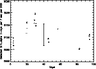
Figure 4: Stability of HEXS for silicon K detection over time.
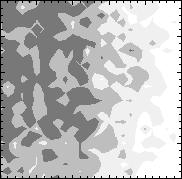
Figure 5: Uniformity of HEXS silicon K detection across CCD.
The x-ray flux from HEXS is remarkably steady, particularly when
operated at low power (less than 6 W). Figure 4 shows a cumulative
plot of about half the data taken to date of the K flux rate from a
silicon target, with a respective constant tube voltage and current of
15 kV and 260
flux rate from a
silicon target, with a respective constant tube voltage and current of
15 kV and 260  A. The entire data set was taken with the same CCD
over a period of nearly 100 days, in six subsets. Each diamond
represents the average flux of detected silicon K
A. The entire data set was taken with the same CCD
over a period of nearly 100 days, in six subsets. Each diamond
represents the average flux of detected silicon K x-rays
taken over 600 exposures of 7.15 seconds duration. The error bar
represents
x-rays
taken over 600 exposures of 7.15 seconds duration. The error bar
represents  standard deviation of all data points. Clearly
the standard deviation is smaller within each subset. Thus the
calibration accuracy is limited by source stability over periods of an
hour or less.
standard deviation of all data points. Clearly
the standard deviation is smaller within each subset. Thus the
calibration accuracy is limited by source stability over periods of an
hour or less.
A second characteristic of interest is the uniformity of the x-ray
beam across the CCD. Figure 5 shows this variation in a grey scale
plot. The data set represents about 65 million silicon K photons collected over the entire CCD during 84,000 seconds. The AXAF
ACIS CCDs have a 1024 x 1024 pixel arrangement, but the data is
rebinned into a 32 x 32 pixel array to optimize presentation.
Quantitatively, the grey scale range from white to darkest corresponds
to 0.990, 0.995, 1.000, and 1.005 times the average flux taken over
the entire CCD. It is not clear whether this variation is due to
either the CCD or the x-ray source. Note that the silicon target is
about 70 cm away during this measurement, giving an expected
point-source cosine variation of 0.0002, far less than that observed.
photons collected over the entire CCD during 84,000 seconds. The AXAF
ACIS CCDs have a 1024 x 1024 pixel arrangement, but the data is
rebinned into a 32 x 32 pixel array to optimize presentation.
Quantitatively, the grey scale range from white to darkest corresponds
to 0.990, 0.995, 1.000, and 1.005 times the average flux taken over
the entire CCD. It is not clear whether this variation is due to
either the CCD or the x-ray source. Note that the silicon target is
about 70 cm away during this measurement, giving an expected
point-source cosine variation of 0.0002, far less than that observed.
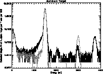
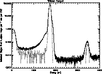
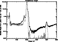
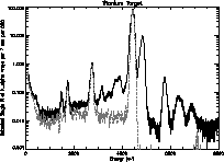
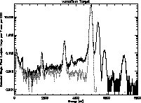
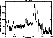
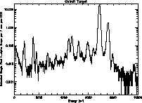
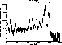
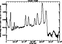
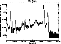
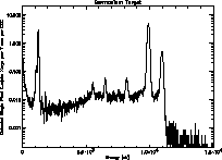
The spectra from 12 different targets used in the calibration are presented in Figs. 6 - 17. All these spectra are from the same CCD (I.D. w102c3) and are cumulative spectra from all data taken over a 100 day period. All the spectra include only x-rays detected in one quadrant (which corresponds to a single analogue-to-digital amplifier chain), although the presented flux rate is multiplied by four to easily indicate flux over the entire chip. There are many features worthy of comment, but only a few will be mentioned.
The first six spectra (Figs. 6 - 11) are overlaid with a lightly dotted spectra, which is that from an x-ray monochromator at the PTB laboratory[5] at the BESSY synchrotron source using the same CCD. The synchrotron beam is passed through a double crystal monochromator producing a highly monochromatic x-ray beam with variable energies and high resolution. Due to the purity of the beam, these spectra are the clearest representation of the CCD response. A full presentation of the BESSY analysis will be presented elsewhere.
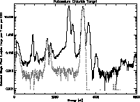
Figure 9: Potassium Chloride Target.
Comparing the spectra reveals impurities in the HEXS beam from either
scattered x-rays or other atomic processes. One example is seen in
the low energy tail of the main photopeak of Fig. 7. Figures 7 and 8
also nicely show the K line lacking in the synchrotron
spectra. Another difference at 520 eV in Fig. 11 is due to the L line
of vanadium. There is also a large difference above the main peak,
seen best in Fig. 8, due to Compton scattering from the target.
Lastly, Fig. 10 shows anomalous lines around 3500 eV which are due to
diffraction effects from the target (to be discussed later). Note
that the large difference seen with the potassium chloride target of
Fig. 9 is due the combined spectra from each element of K and Cl.
Only the BESSY spectrum from potassium is shown for the reason of
clarity. In general, the spectrum from each HEXS target should include
a main K
line lacking in the synchrotron
spectra. Another difference at 520 eV in Fig. 11 is due to the L line
of vanadium. There is also a large difference above the main peak,
seen best in Fig. 8, due to Compton scattering from the target.
Lastly, Fig. 10 shows anomalous lines around 3500 eV which are due to
diffraction effects from the target (to be discussed later). Note
that the large difference seen with the potassium chloride target of
Fig. 9 is due the combined spectra from each element of K and Cl.
Only the BESSY spectrum from potassium is shown for the reason of
clarity. In general, the spectrum from each HEXS target should include
a main K , a smaller K
 , a Si escape peak, and a
silicon peak. The low energy rise seen in every spectrum is not due to
electronic noise, but is a real feature of the CCD response due to
boundaries of the detecting silicon region and the gate structure. The
details of the CCD response are described elsewhere.
, a Si escape peak, and a
silicon peak. The low energy rise seen in every spectrum is not due to
electronic noise, but is a real feature of the CCD response due to
boundaries of the detecting silicon region and the gate structure. The
details of the CCD response are described elsewhere.
No comparative BESSY spectra were taken for the targets illustrated in
Figs. 12 - 17 due to energy limitations of the reflecting grating
monochromator. Many of the lines seen in the high Z target spectra are not
due to impurities or the escape peaks, but are from the following
diffraction process. Most of the high Z targets are metals which
present a polycrystalline matrix at the surface. The target is a flat
sample oriented at 45 with respect to the CCD and the
molybdenum tube. Thus, when a white light x-ray beam is incident on
the target, there will statistically be some crystal grains on exposed
surface oriented exactly so the Bragg diffraction condition is meet
for some specific energy. If x-rays of this energy are included in the
incident white light beam, they will be coherently scattered towards
the CCD and superimposed on the spectrum. These extra lines can be
useful for obtaining the gain variation with energy. One common
impurity line seen is that of iron, due to scattering from the vacuum
chamber walls. One interesting line to note is the L line, which grows
in prominence with Z, seen best in Fig. 17.
with respect to the CCD and the
molybdenum tube. Thus, when a white light x-ray beam is incident on
the target, there will statistically be some crystal grains on exposed
surface oriented exactly so the Bragg diffraction condition is meet
for some specific energy. If x-rays of this energy are included in the
incident white light beam, they will be coherently scattered towards
the CCD and superimposed on the spectrum. These extra lines can be
useful for obtaining the gain variation with energy. One common
impurity line seen is that of iron, due to scattering from the vacuum
chamber walls. One interesting line to note is the L line, which grows
in prominence with Z, seen best in Fig. 17.