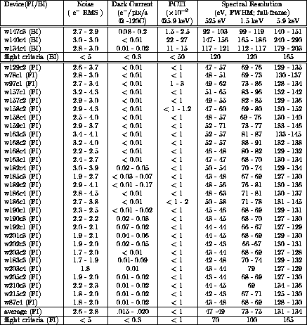
Table 4: ACIS Flight CCD Screening Results
Table 4 lists the devices (and their performance parameters) that meet the minimum screening criteria. In an attempt to simplify the presentation of the results, we do not include data for each output node, but rather give either an upper limit or a range of values.
Upon inspection two features become quite obvious: 1) The BI devices have much poorer energy resolution and higher CTI than the FI devices. Due to their increased quantum efficiency at low energies, BI devices are still being considered as potential ACIS-S detectors. [5] 2) The first ten FI CCDs (w129c2-w168c2) have noise values a few electrons higher than the other CCDs. This property is actually due to the electronics used and is not inherent to the devices. Flight-like electronics, with better performance than standard laboratory electronics, were used starting with device w163c1.

Table 4: ACIS Flight CCD Screening Results
Most of the CCDs easily meet all the acceptance criteria, the only exception being a few devices that have noise levels that are less than one electron RMS from the threshold value. Comparing the spectral resolution measurements with the calculated values presented in Section 4.1.4 reveals that many devices are within 10 % of the theoretical limits. In practice, ranking of devices for calibration turned heavily on spectral resolution at 525 eV and on cosmetic properties. The most common cosmetic problem observed is the defective column. Typically, 2-3 defective columns are present, though a few devices have no defective columns, and one devices has as many as 15 column defects.
It is beyond the scope of this paper to discuss the performance of each device. Instead, we present data on one device that is representative of all flight quality CCDs. Figure 2 is the screening report for CCD c17-185-3 and contains all the measured device parameters.
Figure 3 shows the noise histogram and Gaussian fits for CCD c17-185-3. This device has the common trait of having lower noise in the over-clock region (OC in the plot) than in the image area (IM in the plot). The tails present in nodes c1 and c3 are representative of the shapes and sizes of non-Gaussian deviations that occur during noise characterization measurements. Generally, the histograms are accurately Gaussian over a range of four orders of magnitude.
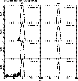
Figure 3: Noise Histograms for c17-185-3
Figure 4 shows the data used in measuring the parallel CTI at
5.9 keV. Following Janesick, pulse height is plotted versus CCD row number, and a line
of the form  is fit to the data.[7] Section
3.4 details this measurement.
The O  , Al
, Al  ,
and
,
and  Fe spectra from the same device are shown in
figures 5, 6, and
7.
The pulse heights range
from 0 to 1700 ADU (analog-to-digital units) to permit a relative comparison of the
spectral resolution at different energies.
A consequence of each output having a different amplifier chain, and hence,
a different gain is that the peaks occur at different ADU values for each
node. The main oxygen peak lies at roughly 100 ADU. The higher energy
features result from pile-up and non-suppressed 2nd and 3rd order
photons produced by the monochromator. Besides the Mn
  and Mn
  lines, the
  Fe spectra contains two other features.
The line at about 1000 ADU is the Si K
 escape
peak. The line at about 1300 ADU is a chromium fluorescence line
produced when Mn X-rays scatter off the stainless steel vacuum tube of the test
system.
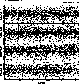
Figure 4: Parallel CTI determination from Mn K
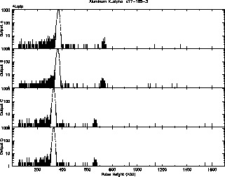
Figure 6: Al  Spectra--1.487 keV
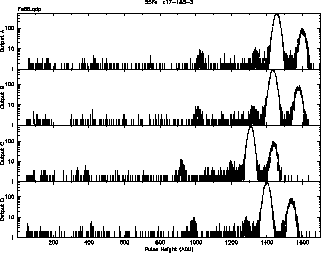
Figure 7:  Fe Spectra--5.898 keV