

Next: 3 Calibration Strategy
Up: X-ray CCD Calibration for
Previous: 1 INTRODUCTION
The ACIS focal plane contains ten MIT Lincoln Laboratory CCID17 detectors.
The CCID17 is a three-phase, frame transfer imager with
1026 rows of 1024 columns in each of the imaging and framestore areas.
The pixels in the imaging area are 24 microns square.
The device is served by four output
nodes which are (usually) operated in parallel. ACIS flight
detectors are fabricated of high-resistivity silicon
( ) to maximize depletion depth and, therefore,
high-energy X-ray detection efficiency. Flight CCDs have been fabricated in
both front-illuminated and back-illuminated configurations. In this paper,
we confine our discussion to the front-illuminated devices.
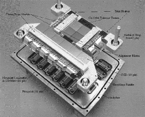
The engineering model ACIS focal plane is shown in
Figure 1. The focal plane consists of ten detectors,
organized into two arrays. The devices in the 2-chip-by-2 chip
ACIS-I array are intended primarily
for high-angular resolution, wide-field imaging, and are therefore tilted to
conform as nearly as possible to the highly-curved focal surface of the AXAF
High-Resolution Mirror Assembly. The linear, 6-chip-long ACIS-S
array is intended primarily for use with the AXAF High-energy Transmission
Gratings (HETG) [8]. The ACIS-S detectors are oriented to conform to the
Rowland circle of the HETG. The gaps between adjacent CCDs are typically 300 microns wide, and are in no case more than 500 microns
wide. In orbit, the focal plane is radiatively cooled to a temperature of
-120 C. This relatively low temperature minimizes the sensitivity of the
detectors to damage from energetic protons encountered on-orbit.

Figure 1: The ACIS CCD focal plane. The ten CCD detectors are arranged in
two subarrays. The 2-by-2 detector subarray supports wide-field imaging.
The 1-by-6 detector subarray supports transmission grating spectroscopy
and narrow-field imaging. The engineering model is shown here; the flight
detector configuration is identical.
The ACIS focal plane is served by a low-noise ( RMS) detector
electronics assembly which contains a dedicated signal chain for
each of the 40 CCD output nodes in the focal plane. Each signal chain
operates at a rate of 100 kpixels s
 , allowing a full detector readout in
less than 3 seconds. The clock sequences produced by the detector
electronics are programmable, so a variety of CCD readout modes are available.
Raw digital data from the detector electronics passes to a high-throughput
digital processing assembly which can service as many of six operating
CCDs simultaneously. The digital processing hardware and software
determine the CCD bias (energy zero-point) level
on a pixel by pixel basis, extract X-ray event information from the incoming
data stream, and format and buffer that data for telemetry to the ground.
ACIS requires optical blocking filters to reject out-of-band radiation
(mainly optical and UV light). Calibration of these filters, which is a critical
part of the ACIS calibration program, is described elsewhere. [9,10]


Next: 3 Calibration Strategy
Up: X-ray CCD Calibration for
Previous: 1 INTRODUCTION
mwb@space.mit.edu
 ) to maximize depletion depth and, therefore,
high-energy X-ray detection efficiency. Flight CCDs have been fabricated in
both front-illuminated and back-illuminated configurations. In this paper,
we confine our discussion to the front-illuminated devices.

 RMS) detector
electronics assembly which contains a dedicated signal chain for
each of the 40 CCD output nodes in the focal plane. Each signal chain
operates at a rate of 100 kpixels s
 , allowing a full detector readout in
less than 3 seconds. The clock sequences produced by the detector
electronics are programmable, so a variety of CCD readout modes are available.