

Previous Section
Title Page
Next Section
Figure 2: Focal Plane Assembly
The ACIS focal plane is made up of ten frame store Charge Coupled Imaging Devices mounted on a paddle (Figure 2) and housed in the detector assembly (Figure 4). The focal plane is divided into two arrays - an imaging array and a spectroscopy array - as shown in Figure 3. The imaging array consists of four CCDs that are mounted such that they conform as closely as possible to the focal surface of the X-ray optics. The spectroscopy array consists of six CCDs that are mounted so that they conform to the Rowland circle of the HETG grating.
The CCDs are front-side illuminated, three phase, frame transfer devices with on chip low noise output circuitry. The CCD detectors, when incorporated into the ACIS system, will be sensitive to X-rays in the energy range from 0.2 KeV to 10 KeV. Each CCD has an imaging area that is an array of pixels arranged in approximately one thousand rows by one thousand columns. Each CCD also has a frame store area that has the same number of pixels arranged in the same one thousand rows by one thousand columns. A charge image from the imaging area of the CCD can be transferred from the imaging area to the frame store area. Once the image is transferred, the charge image in the frame store area can be clocked out one pixel at a time while a new exposure of the imaging area is being captured (this process is effectively electronic shuttering).
Four output buffer amplifiers are provided on each CCD detector to amplify and buffer the signal from the output of the serial output shift registers. The signal from each buffered output represents the data from one quarter of the columns in the frame store area. Having four output amplifiers for each CCD provides a capability of clocking out and processing pixel data from four outputs simultaneously, thus decreasing the frame rate readout time and increasing the time resolution of the observations.
High resolution spectroscopy using CCDs can only be obtained with extremely low-noise processing of the output video signal in addition to adjusting the parameters of the CCDs to their optimal low noise operating point.
The CCD video waveform essentially consists of three distinct levels at different times during clocking of a pixel. First, the CCD reset gate is driven positive to dump any charge that may be present on the output node. Because there is also capacitive coupling from the reset gate to the output node, the output will be above the "zero level", typically by 300 mV, while the reset gate is active. When the reset gate returns to its low state, the video output will return to the zero level. When the last phase of the serial clock is driven low, the video output drops below the zero level. Capacitive coupling produces a drop of about 100 mV, and any charge present at the serial register output will increase this drop by about 10 micro volts/electron.
Due to thermal noise in the reset FET ("kTC" noise), the zero level for each pixel has an uncertainty of about 0.5 mV. In addition, for reasons that are not understood, CCD output noise is often lower if the reset FET's channel is maintained in a pinched off state. In this "soft reset" operating mode, there is no truly fixed operating potential for the output node: the longer reset is applied, the more electrons are removed from the output node (at a decreasing rate as more charge is removed). In this mode, charge coming in from the channel will influence the zero level for subsequent pixels.
The video zero level is actually about 15 V. This offset must obviously be removed. In addition, for best noise performance, and to suppress the influence of one pixel on the next in soft reset mode, it is necessary to measure and subtract the zero level for each individual pixel from the video ("correlated double sampling").
The correlated double sampler should have a high "common mode rejection ratio" to suppress variations in the video zero level. Measurements of video levels should be performed with as narrow a bandwidth as possible to minimize noise, yet the bandwidth limiting should not cause signal from one pixel to spill into the next. It is difficult to achieve both a high common mode rejection ratio and careful bandwidth control in a single circuit, so we perform the zero level subtraction in two steps.
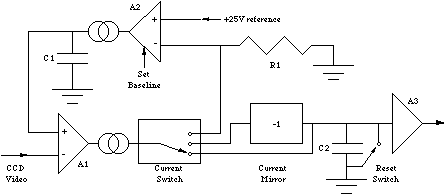 Figure 3: Current Integrating Video Processor
The first step is a fast, wide bandwidth (thus noisy) circuit with a high common mode rejection ratio (Figure 3). Immediately after the CCD reset pulse is removed, the current switch is placed in its upper position and gated transconductance amplifier A2 is activated. This closes a feedback loop that drives the voltage across R1 to the 2.5 V reference voltage, charging C1 to approximately the video zero level. Once this circuit has settled (1 microsecond), A2 is gated off, freezing the voltage on C1. Due to noise, the level to which C1 will settle is uncertain by an amount that is typically 100 micro volts. The common mode rejection ratio is mainly determined by differential transconductance amplifier A1: we use a discrete differential amplifier with a common mode rejection ratio of about 100,000.
Once a rough video zero level is established on C1, the current switch is placed in its middle position. Current from A1 is applied to the current mirror, whose output discharges C2. The voltage on C2 will ramp down at a rate that depends on the current from A1 at the video zero level. The "de-integration" time here is typically 6 microseconds. After de-integration, the final CCD clock phase drives charge into the CCD output node. At the same time, the current switch is placed in its lower position. The current from A1 now charges C2 directly, for an integration time equal to the de-integration time. C2 is left containing an amount of charge that is proportional to the difference between the video zero level and the level to which the CCD clock drove the video. Because it is difficult to make the current mirror gain precisely -1, the common mode rejection ratio of this process is typically only about 50. The resulting errors are negligible, though, because nearly all of the common mode signal has already been rejected.
The current integrator implements a "differential average" filter: this filter is optimal for rejecting white noise from the CCD, and also nearly optimal for rejecting 1/f noise.
In circuit simulations, this video processor shows common mode rejection and rejection of previous pixel of > 10,000. It has intrinsic noise of about 5 micro volts relative to input, which is negligible compared to the approximately 30 micro volt output noise of the CCD. This performance is achieved with a power consumption of about 25 milliwatts. There is a well known noise/power tradeoff in systems like this: low noise generally requires relatively high power because shot noise in amplifiers is relatively reduced by increasing the operating current. The low power consumption of this circuit is a result of the use of current switching: once generated, a current can be switched at little cost in power and noise. The simplicity of the circuit minimizes the number of noise sources and power sinks.